- 您现在的位置:买卖IC网 > PDF目录382630 > TMP320C2811PGFA (Texas Instruments, Inc.) TV 22C 22#22D SKT RECP R&D PDF资料下载
参数资料
| 型号: | TMP320C2811PGFA |
| 厂商: | Texas Instruments, Inc. |
| 英文描述: | TV 22C 22#22D SKT RECP R&D |
| 中文描述: | TMS320R2811,TMS320R2812数字信号处理器 |
| 文件页数: | 59/147页 |
| 文件大小: | 2021K |
| 代理商: | TMP320C2811PGFA |
第1页第2页第3页第4页第5页第6页第7页第8页第9页第10页第11页第12页第13页第14页第15页第16页第17页第18页第19页第20页第21页第22页第23页第24页第25页第26页第27页第28页第29页第30页第31页第32页第33页第34页第35页第36页第37页第38页第39页第40页第41页第42页第43页第44页第45页第46页第47页第48页第49页第50页第51页第52页第53页第54页第55页第56页第57页第58页当前第59页第60页第61页第62页第63页第64页第65页第66页第67页第68页第69页第70页第71页第72页第73页第74页第75页第76页第77页第78页第79页第80页第81页第82页第83页第84页第85页第86页第87页第88页第89页第90页第91页第92页第93页第94页第95页第96页第97页第98页第99页第100页第101页第102页第103页第104页第105页第106页第107页第108页第109页第110页第111页第112页第113页第114页第115页第116页第117页第118页第119页第120页第121页第122页第123页第124页第125页第126页第127页第128页第129页第130页第131页第132页第133页第134页第135页第136页第137页第138页第139页第140页第141页第142页第143页第144页第145页第146页第147页
Peripherals
59
June 2004
SPRS257
Result Registers
EVB
S/W
ADCSOC
EVA
S/W
Sequencer 2
Sequencer 1
SOC
SOC
ADC Control Registers
70B7h
70B0h
70AFh
70A8h
Result Reg 15
Result Reg 8
Result Reg 7
Result Reg 1
Result Reg 0
Module
ADC
12-Bit
Analog
MUX
ADCINA0
ADCINA7
ADCINB0
ADCINB7
System
Control Block
High-Speed
Prescaler
HSPCLK
ADCENCLK
C28x
SYSCLKOUT
S/H
S/H
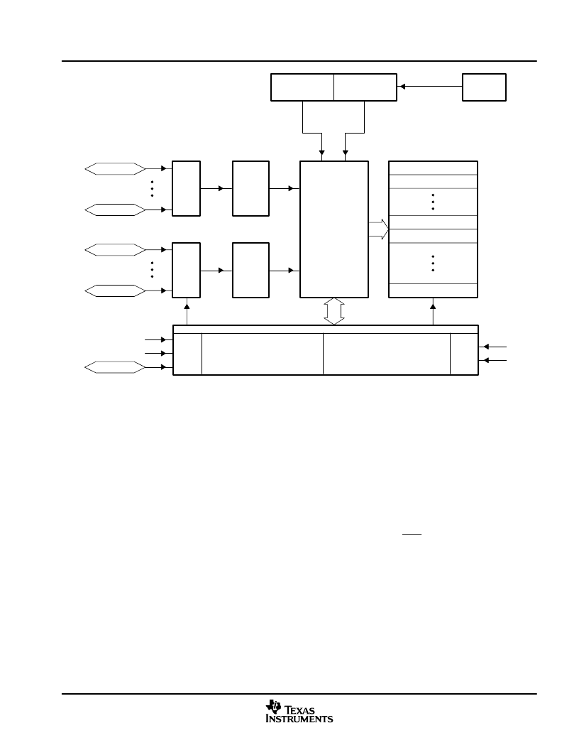
Figure 4
4. Block Diagram of the R281x ADC Module
To obtain the specified accuracy of the ADC, proper board layout is very critical. To the best extent possible,
traces leading to the ADCIN pins should not run in close proximity to the digital signal paths. This is to minimize
switching noise on the digital lines from getting coupled to the ADC inputs. Furthermore, proper isolation
techniques must be used to isolate the ADC module power pins (V
DDA1
/V
DDA2
, AV
DDREFBG
) from the digital
supply. Figure 4
5 shows the ADC pin connections for R281x devices.
Notes:
1.
The ADC registers are accessed at the SYSCLKOUT rate. The internal timing of the ADC module is
controlled by the high-speed peripheral clock (HSPCLK).
2.
The behavior of the ADC module based on the state of the ADCENCLK and HALT signals is as follows:
ADCENCLK:
On reset, this signal will be low. While reset is active-low (XRS) the clock to the register will
still function. This is necessary to make sure all registers and modes go into their default reset state. The
analog module will however be in a low-power inactive state. As soon as reset goes high, then the clock to
the registers will be disabled. When the user sets the ADCENCLK signal high, then the clocks to the
registers will be enabled and the analog module will be enabled. There will be a certain time delay (ms
range) before the ADC is stable and can be used.
HALT:
This signal only affects the analog module. It does not affect the registers. If low, the ADC module is
powered. If high, the ADC module goes into low-power mode. The HALT mode will stop the clock to the
CPU, which will stop the HSPCLK. Therefore the ADC register logic will be turned off indirectly.
Figure 4
5 shows the ADC pin-biasing for internal reference and Figure 4
6 shows the ADC pin-biasing for
external reference.
A
相关PDF资料 |
PDF描述 |
|---|---|
| TMP320C2812PBKA | TMS320R2811, TMS320R2812 Digital Signal Processors |
| TMP320F2812ZHHS | TMS320R2811, TMS320R2812 Digital Signal Processors |
| TMP320R2811PBKA | TMS320R2811, TMS320R2812 Digital Signal Processors |
| TMP320R2811PGFA | TMS320R2811, TMS320R2812 Digital Signal Processors |
| TMS-WINTOTAL-SWARE | SOFTWARE TMS MARKER |
相关代理商/技术参数 |
参数描述 |
|---|---|
| TMP320C2811PGFQ | 制造商:TI 制造商全称:Texas Instruments 功能描述:TMS320R2811, TMS320R2812 Digital Signal Processors |
| TMP320C2811PGFS | 制造商:TI 制造商全称:Texas Instruments 功能描述:TMS320R2811, TMS320R2812 Digital Signal Processors |
| TMP320C2811ZHHA | 制造商:TI 制造商全称:Texas Instruments 功能描述:TMS320R2811, TMS320R2812 Digital Signal Processors |
| TMP320C2811ZHHQ | 制造商:TI 制造商全称:Texas Instruments 功能描述:TMS320R2811, TMS320R2812 Digital Signal Processors |
| TMP320C2811ZHHS | 制造商:TI 制造商全称:Texas Instruments 功能描述:TMS320R2811, TMS320R2812 Digital Signal Processors |
发布紧急采购,3分钟左右您将得到回复。