- 您现在的位置:买卖IC网 > PDF目录382635 > TMS29F800B-90BDCDL (Texas Instruments, Inc.) 1048576 BY 8-BIT/ 524288 BY 16-BIT FLASH MEMORIES PDF资料下载
参数资料
| 型号: | TMS29F800B-90BDCDL |
| 厂商: | Texas Instruments, Inc. |
| 英文描述: | 1048576 BY 8-BIT/ 524288 BY 16-BIT FLASH MEMORIES |
| 中文描述: | 1048576 8位/ 524288由16位闪存 |
| 文件页数: | 17/51页 |
| 文件大小: | 685K |
| 代理商: | TMS29F800B-90BDCDL |
第1页第2页第3页第4页第5页第6页第7页第8页第9页第10页第11页第12页第13页第14页第15页第16页当前第17页第18页第19页第20页第21页第22页第23页第24页第25页第26页第27页第28页第29页第30页第31页第32页第33页第34页第35页第36页第37页第38页第39页第40页第41页第42页第43页第44页第45页第46页第47页第48页第49页第50页第51页
TMS29F800T, TMS29F800B
1048576 BY 8-BIT/524288 BY 16-BIT
FLASH MEMORIES
SMJS835B – MAY 1997 – REVISED OCTOBER 1997
17
POST OFFICE BOX 1443
HOUSTON, TEXAS 77251–1443
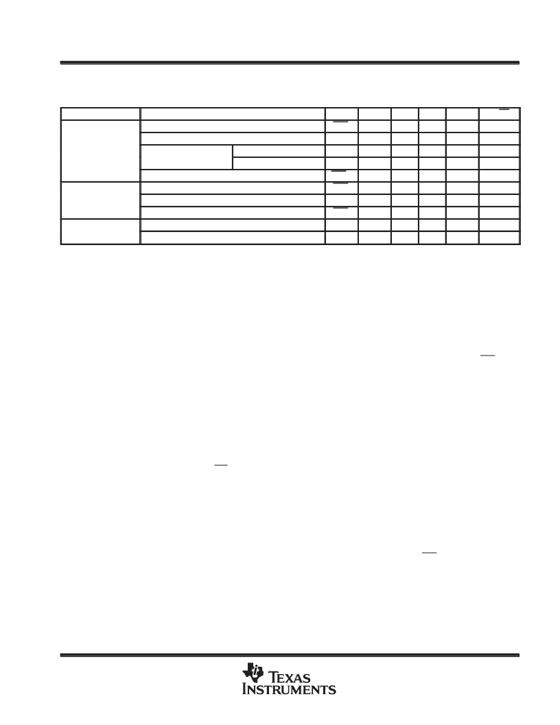
status-bit definitions (continued)
Table 7. Operation Status Flags
DEVICE OPERATION
DQ7
DQ7
DQ6
T
DQ5
0
DQ3
0
DQ2
No Tog
§
RY/BY
0
Programming
Program/erase in auto-erase
0
T
0
1
0
In progress
Erase suspend mode
Erase-suspend mode
Erase-sector address
1
No Tog
0
0
T
1
Non-erase sector address
D
D
D
D
D
1§
1
Program in erase suspend
DQ7
T
0
0
0
Programming
DQ7
T
1
0
No Tog
#
0
Exceeded time limits
Program/erase in auto erase
0
T
1
1
0
Program in erase suspend
DQ7
T
1
0
No Tog
0
Successful operation
complete
Programming complete
D
D
D
D
D
1
Sector-/chip-erase complete
1
1
1
1
1
1
T= toggle, D= data, No Tog= No toggle
DQ4, DQ1, DQ0 are reserved for future use.
§DQ2 can be toggled when the sector address applied is an erasing sector. DQ2 cannot be toggled when the sector address applied is a
non-erasing sector. DQ2 is used to determine which sectors are erasing and which are not.
Status flags apply when outputs are read from the address of a non-erase-suspend operation.
#If DQ5 is high (exceeded timing limits), successive reads from a problem sector causes DQ2 to toggle.
data-polling (DQ7)
The data-polling-status function outputs the complement of the data latched into the DQ7 data register while
the write-state machine (WSM) is engaged in a program or erase operation. Data bit DQ7 changes from
complement to true to indicate the end of an operation. Data-polling is available only during programming,
chip-erase, sector-erase, and sector-erase-timing delay. Data-polling is valid after the rising edge of WE in the
last bus cycle of the command sequence loaded into the command register. Figure 16 shows a flowchart for
data-polling.
During a program operation, reading DQ7 outputs the complement of the DQ7 data to be programmed at the
selected address location. Upon completion, reading DQ7 outputs the true DQ7 data loaded into the
program-data register. During the erase operations, reading DQ7 outputs a logic low. Upon completion, reading
DQ7 outputs a logic high. Also, data-polling must be performed at a sector address that is within a sector that
is being erased. Otherwise, the status is invalid. When using data-polling, the address should remain stable
throughout the operation.
During a data-polling read, while OE is logic low, data bit DQ7 can change asynchronously. Depending on the
read timing, the system can read valid data on DQ7, while other DQ pins are still invalid. A subsequent read
of the device is valid. See Figure 17 for the data-polling timing diagram.
toggle bit (DQ6)
The toggle-bit status function outputs data on DQ6, which toggles between logic high and logic low while the
WSM is engaged in a program or erase operation. When DQ6 stops toggling after two consecutive reads to the
same address, the operation is complete. The toggle bit is available only during programming, chip erase, sector
erase, and sector-erase-timing delay. Toggle-bit data is valid after the rising edge of WE in the last bus cycle
of the command sequence loaded into the command register. Figure 18 shows a flowchart of the toggle-bit
status-read algorithm. Depending on the read timing, DQ6 can stop toggling while other DQ pins are still invalid
and a subsequent read of the device is valid. See Figure 19 for the toggle-bit timing diagram.
P
相关PDF资料 |
PDF描述 |
|---|---|
| TMS29F800B-100BDCDE | 1048576 BY 8-BIT/ 524288 BY 16-BIT FLASH MEMORIES |
| TMS29F800B-100BDCDL | 1048576 BY 8-BIT/ 524288 BY 16-BIT FLASH MEMORIES |
| TMS29F800B-100BDCDQ | PT 8C 8#20 PIN RECP |
| TMS29F800B-100CDBJE | RECEPT |
| TMS29F800B-100CDBJL | 1048576 BY 8-BIT/ 524288 BY 16-BIT FLASH MEMORIES |
相关代理商/技术参数 |
参数描述 |
|---|---|
| TMS29F81606FML | 制造商:TI 功能描述:* |
| TMS-3/16-1.50-2 | 制造商:TE Connectivity 功能描述:5021710001 |
| TMS-3/16-1.50-3 | 制造商:TE Connectivity 功能描述:5023130001 |
| TMS-3/16-1.50-4 | 功能描述:电线鉴定 TMS-3/16-1.50-4 RoHS:否 制造商:TE Connectivity / Q-Cees 产品:Labels and Signs 类型: 材料:Vinyl 颜色:Blue 宽度:0.625 in 长度:1 in |
| TMS-3/16-1.50-4-CS7290 | 制造商:TE Connectivity 功能描述:502094N002 |
发布紧急采购,3分钟左右您将得到回复。