- 您现在的位置:买卖IC网 > PDF目录382635 > TMS320C241FNS 16-Bit Digital Signal Processor PDF资料下载
参数资料
| 型号: | TMS320C241FNS |
| 元件分类: | 数字信号处理 |
| 英文描述: | 16-Bit Digital Signal Processor |
| 中文描述: | 16位数字信号处理器 |
| 文件页数: | 12/116页 |
| 文件大小: | 1485K |
| 代理商: | TMS320C241FNS |
第1页第2页第3页第4页第5页第6页第7页第8页第9页第10页第11页当前第12页第13页第14页第15页第16页第17页第18页第19页第20页第21页第22页第23页第24页第25页第26页第27页第28页第29页第30页第31页第32页第33页第34页第35页第36页第37页第38页第39页第40页第41页第42页第43页第44页第45页第46页第47页第48页第49页第50页第51页第52页第53页第54页第55页第56页第57页第58页第59页第60页第61页第62页第63页第64页第65页第66页第67页第68页第69页第70页第71页第72页第73页第74页第75页第76页第77页第78页第79页第80页第81页第82页第83页第84页第85页第86页第87页第88页第89页第90页第91页第92页第93页第94页第95页第96页第97页第98页第99页第100页第101页第102页第103页第104页第105页第106页第107页第108页第109页第110页第111页第112页第113页第114页第115页第116页
TMS320F243, TMS320F241
DSP CONTROLLERS
SPRS064B – DECEMBER 1997 – REVISED FEBRUARY 1999
12
POST OFFICE BOX 1443
HOUSTON, TEXAS 77251–1443
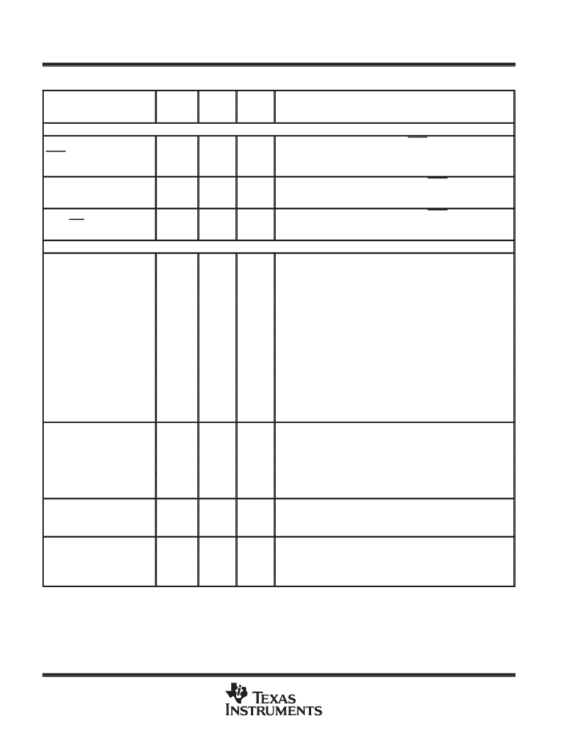
Terminal Functions - ’F243 PGE Package (Continued)
NAME
144
QFP
NO.
TYPE
RESET
STATE
DESCRIPTION
TEST SIGNALS (CONTINUED)
TRST
30
I
I
JTAG test reset with internal pulldown. TRST, when driven high, gives
the scan system control of the operations of the device. If this signal is
not connected or driven low, the device operates in its functional mode,
and the test reset signals are ignored.
EMU0
45
I/O
I
Emulator I/O pin 0 with internal pullup. When TRST is driven high, this
pin is used as an interrupt to or from the emulator system and is defined
as input/output through the JTAG scan.
EMU1/OFF
47
I/O
I
Emulator I/O pin 1 with internal pullup. When TRST is driven high, this
pin is used as an interrupt to or from the emulator system and is defined
as input/output through JTAG scan.
SUPPLY SIGNALS
14
15
36
37
40
70
VSSO
73
–
–
Digital logic and buffer ground reference
108
111
117
124
129
131
34
39
VDDO
72
Digital logic and buffer supply voltage
75
–
–
106
109
17
VDD
53
–
–
Digital logic supply voltage
125
16
VSS
32
Digital logic ground reference
51
127
–
–
I = input, O = output, Z = high impedance
The reset state indicates the state of the pin at reset. If the pin is an input, indicated by an I, its state is determined by user design. If the pin is
an output, its level at reset is indicated.
§ In silicon revisions 2.0-TMX and 2.1-TMS, this pin is level-sensitive and can cause multiple interrupts when held low.
Data is in output mode when AVIS is enabled. At reset, the device comes up with AVIS mode enabled. The data bus is in output mode while AVIS
is enabled.
NOTE:
Bold, italicized pin names
indicate pin function after reset.
相关PDF资料 |
PDF描述 |
|---|---|
| TMS320C241PGS | 16-Bit Digital Signal Processor |
| TMS320F241FNQ | 16-Bit Digital Signal Processor |
| TMS320F241PGQ | 16-Bit Digital Signal Processor |
| TMS320F243PGEQ | 16-Bit Digital Signal Processor |
| TMS320F243PGES | 16-Bit Digital Signal Processor |
相关代理商/技术参数 |
参数描述 |
|---|---|
| TMS320C241PGS | 制造商:未知厂家 制造商全称:未知厂家 功能描述:16-Bit Digital Signal Processor |
| TMS320C242 | 制造商:TI 制造商全称:Texas Instruments 功能描述:DSP CONTROLLER |
| TMS320C242FN | 制造商:TI 制造商全称:Texas Instruments 功能描述:DSP CONTROLLER |
| TMS320C242FNA | 制造商:未知厂家 制造商全称:未知厂家 功能描述:16-Bit Digital Signal Processor |
| TMS320C242FNS | 制造商:未知厂家 制造商全称:未知厂家 功能描述:16-Bit Digital Signal Processor |
发布紧急采购,3分钟左右您将得到回复。