- 您现在的位置:买卖IC网 > PDF目录382641 > TMS320SP5410AGGU12 (Texas Instruments, Inc.) Fixed-Point Digital Signal Processor PDF资料下载
参数资料
| 型号: | TMS320SP5410AGGU12 |
| 厂商: | Texas Instruments, Inc. |
| 元件分类: | 数字信号处理 |
| 英文描述: | Fixed-Point Digital Signal Processor |
| 中文描述: | 定点数字信号处理器 |
| 文件页数: | 14/100页 |
| 文件大小: | 913K |
| 代理商: | TMS320SP5410AGGU12 |
第1页第2页第3页第4页第5页第6页第7页第8页第9页第10页第11页第12页第13页当前第14页第15页第16页第17页第18页第19页第20页第21页第22页第23页第24页第25页第26页第27页第28页第29页第30页第31页第32页第33页第34页第35页第36页第37页第38页第39页第40页第41页第42页第43页第44页第45页第46页第47页第48页第49页第50页第51页第52页第53页第54页第55页第56页第57页第58页第59页第60页第61页第62页第63页第64页第65页第66页第67页第68页第69页第70页第71页第72页第73页第74页第75页第76页第77页第78页第79页第80页第81页第82页第83页第84页第85页第86页第87页第88页第89页第90页第91页第92页第93页第94页第95页第96页第97页第98页第99页第100页
www.ti.com
TMS320VC5410A
Fixed-Point Digital Signal Processor
SPRS139G–NOVEMBER 2000–REVISED JANUARY 2005
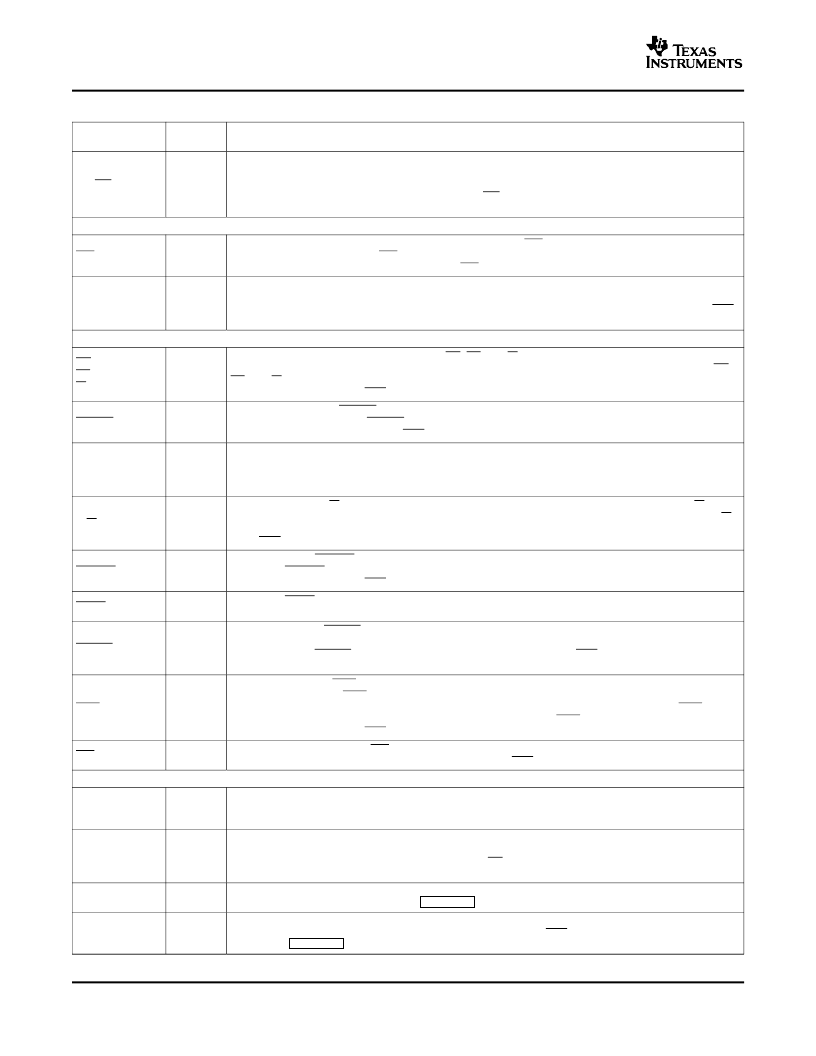
Table 2-2. Signal Descriptions (continued)
TERMINAL
NAME
I/O
(1)
DESCRIPTION
Microprocessor/microcomputer mode select. If active low at reset, microcomputer mode is selected, and
the internal program ROM is mapped into the upper 16K words of program memory space. If the pin is
driven high during reset, microprocessor mode is selected, and the on-chip ROM is removed from program
space. This pin is only sampled at reset, and the MP/MC bit of the processor mode status (PMST) register
can override the mode that is selected at reset.
MULTIPROCESSING SIGNALS
Branch control. A branch can be conditionally executed when BIO is active. If low, the processor executes
the conditional instruction. The BIO condition is sampled during the decode phase of the pipeline for the
XC instruction, and all other instructions sample BIO during the read phase of the pipeline.
External flag output (latched software-programmable signal). XF is set high by the SSBX XF instruction, set
low by RSBX XF instruction or by loading ST1. XF is used for signaling other processors in multiprocessor
configurations or used as a general-purpose output pin. XF goes into the high-impedance state when OFF
is low, and is set high at reset.
MEMORY CONTROL SIGNALS
Data, program, and I/O space select signals. DS, PS, and IS are always high unless driven low for
communicating to a particular external space. Active period corresponds to valid address information. DS,
PS, and IS are placed into the high-impedance state in the hold mode; these signals also go into the
high-impedance state when OFF is low.
Memory strobe signal. MSTRB is always high unless low-level asserted to indicate an external bus access
to data or program memory. MSTRB is placed in the high-impedance state in the hold mode; it also goes
into the high-impedance state when OFF is low.
Data ready. READY indicates that an external device is prepared for a bus transaction to be completed. If
the device is not ready (READY is low), the processor waits one cycle and checks READY again. Note that
the processor performs ready detection if at least two software wait states are programmed. The READY
signal is not sampled until the completion of the software wait states.
Read/write signal. R/W indicates transfer direction during communication to an external device. R/W is
normally in the read mode (high), unless it is asserted low when the DSP performs a write operation. R/W
is placed in the high-impedance state in the hold mode; and it also goes into the high-impedance state
when OFF is low.
I/O strobe signal. IOSTRB is always high unless low-level asserted to indicate an external bus access to an
I/O device. IOSTRB is placed in the high-impedance state in the hold mode; it also goes into the
high-impedance state when OFF is low.
Hold input. HOLD is asserted to request control of the address, data, and control lines. When
acknowledged by the 5410A, these lines go into the high-impedance state.
Hold acknowledge. HOLDA indicates to the external circuitry that the processor is in a hold state and that
the address, data, and control lines are in the high-impedance state, allowing them to be available to the
external circuitry. HOLDA also goes into the high-impedance state when OFF is low. This pin is driven high
during reset.
Microstate complete. MSC indicates completion of all software wait states. When two or more software wait
states are enabled, the MSC pin goes active at the beginning of the first software wait state and goes
inactive high at the beginning of the last software wait state. If connected to the READY input, MSC forces
one external wait state after the last internal wait state is completed. MSC also goes into the
high-impedance state when OFF is low.
Instruction acquisition signal. IAQ is asserted (active low) when there is an instruction address on the
address bus and goes into the high-impedance state when OFF is low.
TIMER SIGNALS
Clock output signal. CLKOUT can represent the machine-cycle rate of the CPU divided by 1, 2, 3, or 4 as
configured in the bank-switching control register (BSCR). Following reset, CLKOUT represents the
machine-cycle rate divided by 4.
Clock mode select signals. CLKMD1-CLKMD3 allow the selection and configuration of different clock
modes such as crystal, external clock, and PLL mode. The external CLKMD1-CLKMD3 pins are sampled
to determine the desired clock generation mode while RS is low. Following reset, the clock generation
mode can be reconfigured by writing to the internal clock mode register in software.
Clock/oscillator input. If the internal oscillator is not being used, X2/CLKIN functions as the clock input.
(This is revision depended, see Section Section 3.6 for additional information.)
Output pin from the internal oscillator for the crystal. If the internal oscillator is not used, X1 should be left
unconnected. X1 does not go into the high-impedance state when OFF is low. (This is revision depended,
see Section Section 3.6 for additional information.)
MP/MC
I
BIO
(2)
I
XF
O/Z
DS
PS
IS
O/Z
MSTRB
O/Z
READY
I
R/W
O/Z
IOSTRB
O/Z
HOLD
I
HOLDA
O/Z
MSC
O/Z
IAQ
O/Z
CLKOUT
O/Z
CLKMD1
(2)
CLKMD2
(2)
CLKMD3
(2)
I
X2/CLKIN
(2)
I
X1
O
14
Introduction
相关PDF资料 |
PDF描述 |
|---|---|
| TMS320SP5410AZGU12 | Fixed-Point Digital Signal Processor |
| TMS32C6411ZLZA6E3 | FIXED-POINT DIGITAL SIGNAL PROCESSORS |
| TMS32C6416EGLSA6E3 | FIXED-POINT DIGITAL SIGNAL PROCESSORS |
| TMS32C6415CGLSA6E3 | FIXED-POINT DIGITAL SIGNAL PROCESSORS |
| TMS32C6411GLSA6E3 | FIXED-POINT DIGITAL SIGNAL PROCESSORS |
相关代理商/技术参数 |
参数描述 |
|---|---|
| TMS320SP5410AZGU12 | 功能描述:数字信号处理器和控制器 - DSP, DSC Fixed-Point DSP RoHS:否 制造商:Microchip Technology 核心:dsPIC 数据总线宽度:16 bit 程序存储器大小:16 KB 数据 RAM 大小:2 KB 最大时钟频率:40 MHz 可编程输入/输出端数量:35 定时器数量:3 设备每秒兆指令数:50 MIPs 工作电源电压:3.3 V 最大工作温度:+ 85 C 封装 / 箱体:TQFP-44 安装风格:SMD/SMT |
| TMS320SP6713GDP225 | 制造商:Texas Instruments 功能描述:5410PGE-100 100 MIPS 144TQFP REV 2.0 - Trays |
| TMS320SPVC5470GHK | 功能描述:数字信号处理器和控制器 - DSP, DSC Quad Bus Buffer Gate With 3-State Outputs RoHS:否 制造商:Microchip Technology 核心:dsPIC 数据总线宽度:16 bit 程序存储器大小:16 KB 数据 RAM 大小:2 KB 最大时钟频率:40 MHz 可编程输入/输出端数量:35 定时器数量:3 设备每秒兆指令数:50 MIPs 工作电源电压:3.3 V 最大工作温度:+ 85 C 封装 / 箱体:TQFP-44 安装风格:SMD/SMT |
| TMS320SS16FNL | 制造商:Rochester Electronics LLC 功能描述:- Bulk |
| TMS320SS16NL | 制造商:Rochester Electronics LLC 功能描述:- Bulk |
发布紧急采购,3分钟左右您将得到回复。