- 您现在的位置:买卖IC网 > PDF目录19903 > TNY264GN-TL (Power Integrations)IC OFFLINE SWIT OTP OCP HV 8SMD PDF资料下载
参数资料
| 型号: | TNY264GN-TL |
| 厂商: | Power Integrations |
| 文件页数: | 3/22页 |
| 文件大小: | 0K |
| 描述: | IC OFFLINE SWIT OTP OCP HV 8SMD |
| 标准包装: | 1 |
| 输出隔离: | 隔离 |
| 频率范围: | 124kHz ~ 140kHz |
| 输出电压: | 700V |
| 功率(瓦特): | 9W |
| 工作温度: | -40°C ~ 150°C |
| 封装/外壳: | 8-SMD(7 个接脚),鸥形翼 |
| 供应商设备封装: | SMD-8B |
| 包装: | 标准包装 |
| 产品目录页面: | 1203 (CN2011-ZH PDF) |
| 其它名称: | 596-1046-6 |
�� �
�
�TNY263-268�
�TinySwitch-II� Functional� Description�
�TinySwitch-II� combines� a� high� voltage� power� MOSFET� switch�
�with� a� power� supply� controller� in� one� device.� Unlike�
�conventional� PWM� (pulse� width� modulator)� controllers,�
�TinySwitch-II� uses� a� simple� ON/OFF� control� to� regulate� the�
�output� voltage.�
�The� TinySwitch-II� controller� consists� of� an� oscillator,� enable�
�circuit� (sense� and� logic),� current� limit� state� machine,�
�5.8� V� regulator,� BYPASS� pin� undervoltage� circuit,� over-�
�temperature� protection,� current� limit� circuit,� leading� edge�
�blanking� and� a� 700� V� power� MOSFET.� TinySwitch-II�
�incorporates� additional� circuitry� for� line� undervoltage� sense,�
�auto-restart� and� frequency� jitter.� Figure� 2� shows� the� functional�
�block� diagram� with� the� most� important� features.�
�Oscillator�
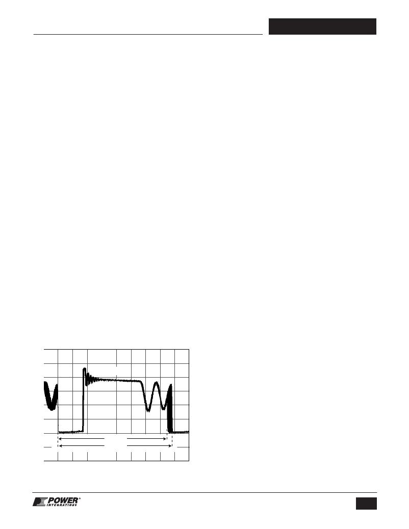
�The� typical� oscillator� frequency� is� internally� set� to� an� average�
�of� 132� kHz.� Two� signals� are� generated� from� the� oscillator:� the�
�maximum� duty� cycle� signal� (DC� MAX� )� and� the� clock� signal� that�
�indicates� the� beginning� of� each� cycle.�
�The� TinySwitch-II� oscillator� incorporates� circuitry� that�
�introduces� a� small� amount� of� frequency� jitter,� typically� 8� kHz�
�peak-to-peak,� to� minimize� EMI� emission.� The� modulation� rate�
�of� the� frequency� jitter� is� set� to� 1� kHz� to� optimize� EMI� reduction�
�for� both� average� and� quasi-peak� emissions.� The� frequency�
�jitter� should� be� measured� with� the� oscilloscope� triggered� at�
�the� falling� edge� of� the� DRAIN� waveform.� The� waveform� in�
�Figure� 4� illustrates� the� frequency� jitter� of� the� TinySwitch-II.�
�Enable� Input� and� Current� Limit� State� Machine�
�The� enable� input� circuit� at� the� EN/UV� pin� consists� of� a� low�
�impedance� source� follower� output� set� at� 1.0� V.� The� current�
�through� the� source� follower� is� limited� to� 240� μ� A.� When� the�
�current� out� of� this� pin� exceeds� 240� μ� A,� a� low� logic� level�
�(disable)� is� generated� at� the� output� of� the� enable� circuit.� This�
�enable� circuit� output� is� sampled� at� the� beginning� of� each� cycle�
�on� the� rising� edge� of� the� clock� signal.� If� high,� the� power�
�MOSFET� is� turned� on� for� that� cycle� (enabled).� If� low,� the� power�
�600�
�MOSFET� remains� off� (disabled).� Since� the� sampling� is� done�
�only� at� the� beginning� of� each� cycle,� subsequent� changes� in�
�the� EN/UV� pin� voltage� or� current� during� the� remainder� of� the�
�cycle� are� ignored.�
�The� current� limit� state� machine� reduces� the� current� limit� by�
�discrete� amounts� at� light� loads� when� TinySwitch-II� is� likely� to�
�switch� in� the� audible� frequency� range.� The� lower� current� limit�
�raises� the� effective� switching� frequency� above� the� audio� range�
�and� reduces� the� transformer� ?ux� density,� including� the�
�associated� audible� noise.� The� state� machine� monitors� the�
�sequence� of� EN/UV� pin� voltage� levels� to� determine� the� load�
�condition� and� adjusts� the� current� limit� level� accordingly� in�
�discrete� amounts.�
�Under� most� operating� conditions� (except� when� close� to� no-�
�load),� the� low� impedance� of� the� source� follower� keeps� the�
�voltage� on� the� EN/UV� pin� from� going� much� below� 1.0� V� in� the�
�disabled� state.� This� improves� the� response� time� of� the�
�optocoupler� that� is� usually� connected� to� this� pin.�
�5.8� V� Regulator� and� 6.3� V� Shunt� Voltage� Clamp�
�The� 5.8� V� regulator� charges� the� bypass� capacitor� connected�
�to� the� BYPASS� pin� to� 5.8� V� by� drawing� a� current� from� the�
�voltage� on� the� DRAIN� pin� whenever� the� MOSFET� is� off.� The�
�BYPASS� pin� is� the� internal� supply� voltage� node� for� the�
�TinySwitch-II.� When� the� MOSFET� is� on,� the� TinySwitch-II�
�operates� from� the� energy� stored� in� the� bypass� capacitor.�
�Extremely� low� power� consumption� of� the� internal� circuitry�
�allows� TinySwitch-II� to� operate� continuously� from� current� it�
�takes� from� the� DRAIN� pin.� A� bypass� capacitor� value� of� 0.1� μ� F�
�is� suf� ?cient� for� both� high� frequency� decoupling� and� energy�
�storage.�
�In� addition,� there� is� a� 6.3� V� shunt� regulator� clamping� the�
�BYPASS� pin� at� 6.3� V� when� current� is� provided� to� the� BYPASS�
�pin� through� an� external� resistor.� This� facilitates� powering� of�
�TinySwitch-II� externally� through� a� bias� winding� to� decrease� the�
�no-load� consumption� to� about� 50� mW.�
�BYPASS� Pin� Undervoltage�
�The� BYPASS� pin� undervoltage� circuitry� disables� the� power�
�MOSFET� when� the� BYPASS� pin� voltage� drops� below� 4.8� V.�
�500�
�V� DRAIN�
�Once� the� BYPASS� pin� voltage� drops� below� 4.8� V,� it� must� rise�
�back� to� 5.8� V� to� enable� (turn-on)� the� power� MOSFET.�
�400�
�300�
�200�
�100�
�0�
�136� kHz�
�Over� Temperature� Protection�
�The� thermal� shutdown� circuitry� senses� the� die� temperature.�
�The� threshold� is� typically� set� at� 135� °� C� with� 70� °� C� hysteresis.�
�When� the� die� temperature� rises� above� this� threshold� the�
�power� MOSFET� is� disabled� and� remains� disabled� until� the� die�
�temperature� falls� by� 70� °� C,� at� which� point� it� is� re-enabled.� A�
�large� hysteresis� of� 70� °� C� (typical)� is� provided� to� prevent�
�overheating� of� the� PC� board� due� to� a� continuous� fault�
�condition.�
�128� kHz�
�Current� Limit�
�The� current� limit� circuit� senses� the� current� in� the� power�
�0�
�Figure� 4.�
�Frequency� Jitter.�
�5�
�Time� (� μ� s)�
�10�
�MOSFET.� When� this� current� exceeds� the� internal� threshold�
�(I� LIMIT� ),� the� power� MOSFET� is� turned� off� for� the� remainder� of�
�3�
�www.powerint.com�
�Rev.� H� 02/09�
�相关PDF资料 |
PDF描述 |
|---|---|
| S101J39SL0P6TK5R | CAP CER 100PF 2KV 5% RADIAL |
| ICL7663SCBA | IC REG LDO ADJ 40MA 8-SOIC |
| LTC4301LCDD | IC BUFFER BUS HOTSWAP 2WR 8DFN |
| R12P212D/P | CONV DC/DC 2W 12VIN +/-12VOUT |
| NCV8503PW33G | IC REG LDO 3.3V .4A 16-SOIC |
相关代理商/技术参数 |
参数描述 |
|---|---|
| TNY264GTL | 制造商:POWERINT 制造商全称:Power Integrations, Inc. 功能描述:Enhanced, Energy Efficient, Low Power Off-line Switcher |
| TNY264G-TL | 功能描述:IC OFFLINE SWIT OTP OCP HV 8SMD RoHS:否 类别:集成电路 (IC) >> PMIC - AC-DC 转换器,离线开关 系列:TinySwitch®-II 标准包装:1 系列:FPS™ 输出隔离:隔离 频率范围:61kHz ~ 73kHz 输入电压:8 V ~ 26 V 输出电压:650V 功率(瓦特):12W 工作温度:-40°C ~ 115°C 封装/外壳:8-DIP(0.300",7.62mm) 供应商设备封装:8-MDIP 包装:Digi-Reel® 其它名称:FSL206MRBNFSDKR |
| TNY264P | 功能描述:IC OFFLINE SWIT OTP OCP HV 8DIP RoHS:否 类别:集成电路 (IC) >> PMIC - AC-DC 转换器,离线开关 系列:TinySwitch®-II 标准包装:1 系列:FPS™ 输出隔离:隔离 频率范围:61kHz ~ 73kHz 输入电压:8 V ~ 26 V 输出电压:650V 功率(瓦特):12W 工作温度:-40°C ~ 115°C 封装/外壳:8-DIP(0.300",7.62mm) 供应商设备封装:8-MDIP 包装:Digi-Reel® 其它名称:FSL206MRBNFSDKR |
| TNY264P_1 | 制造商:POWERINT 制造商全称:Power Integrations, Inc. 功能描述:2.4W Cell Phone Charger |
| TNY264PG | 功能描述:交流/直流开关转换器 6 W (85-265 VAC) 9 W (230 VAC) RoHS:否 制造商:STMicroelectronics 输出电压:800 V 输入/电源电压(最大值):23.5 V 输入/电源电压(最小值):11.5 V 开关频率:115 kHz 电源电流:1.6 mA 工作温度范围:- 40 C to + 150 C 安装风格:SMD/SMT 封装 / 箱体:SSO-10 封装:Reel |
发布紧急采购,3分钟左右您将得到回复。