- 您现在的位置:买卖IC网 > PDF目录68612 > TOP242G-TL (POWER INTEGRATIONS INC) 0.72 A SWITCHING REGULATOR, 140 kHz SWITCHING FREQ-MAX, PDSO7 PDF资料下载
参数资料
| 型号: | TOP242G-TL |
| 厂商: | POWER INTEGRATIONS INC |
| 元件分类: | 稳压器 |
| 英文描述: | 0.72 A SWITCHING REGULATOR, 140 kHz SWITCHING FREQ-MAX, PDSO7 |
| 封装: | PLASTIC, SMD-8/7 |
| 文件页数: | 22/52页 |
| 文件大小: | 2175K |
| 代理商: | TOP242G-TL |
第1页第2页第3页第4页第5页第6页第7页第8页第9页第10页第11页第12页第13页第14页第15页第16页第17页第18页第19页第20页第21页当前第22页第23页第24页第25页第26页第27页第28页第29页第30页第31页第32页第33页第34页第35页第36页第37页第38页第39页第40页第41页第42页第43页第44页第45页第46页第47页第48页第49页第50页第51页第52页
TOP242-250
29
N
4/05
Input Capacitor
Theinputcapacitormustbechosentoprovidetheminimum DC
voltage required for the TOPSwitch-GX converter to maintain
regulation at the lowest specied input voltage and maximum
output power. Since TOPSwitch-GX has a higher DC
MAX than
TOPSwitch-II
, it is possible to use a smaller input capacitor.
ForTOPSwitch-GX,acapacitanceof2Fperwattispossiblefor
universal input with an appropriately designed transformer.
Primary Clamp and Output Reected Voltage V
OR
A primary clamp is necessary to limit the peak TOPSwitch-GX
drain to source voltage. A Zener clamp requires few parts and
takes up little board space. For good efciency, the clamp
Zener should be selected to be at least 1.5 times the output
reectedvoltageV
OR, as this keeps the leakage spike conduction
time short. When using a Zener clamp in a universal input
application, a V
OR of less than 135 V is recommended to allow
for the absolute tolerances and temperature variations of the
Zener. This will ensure efcient operation of the clamp circuit
and will also keep the maximum drain voltage below the rated
breakdown voltage of the TOPSwitch-GX MOSFET.
AhighV
OR is required to take full advantage of the wider DCMAX
of TOPSwitch-GX. An RCD clamp provides tighter clamp
voltage tolerance than a Zener clamp and allows a V
OR as high
as150V. RCDclampdissipationcanbeminimizedbyreducing
the external current limit as a function of input line voltage (see
Figures 21 and 35). The RCD clamp is more cost effective than
the Zener clamp but requires more careful design (see Quick
Design Checklist).
Output Diode
The output diode is selected for peak inverse voltage, output
current, and thermal conditions in the application (including
heatsinking, air circulation, etc.). The higher DC
MAX of
TOPSwitch
-GX, along with an appropriate transformer turns
ratio, can allow the use of a 60 V Schottky diode for higher
efciency on output voltages as high as 15 V (see Figure 41: A
12 V, 30 W design using a 60 V Schottky for the output diode).
Bias Winding Capacitor
Due to the low frequency operation at no-load a 1 F bias
winding capacitor is recommended.
Soft-Start
Generally, a power supply experiences maximum stress at
start-up before the feedback loop achieves regulation. For a
periodof10ms,theon-chipsoft-startlinearlyincreasestheduty
cycle from zero to the default DC
MAX at turn on. In addition,
the primary current limit increases from 85% to 100% over the
same period. This causes the output voltage to rise in an orderly
manner, allowing time for the feedback loop to take control of
the duty cycle. This reduces the stress on the TOPSwitch-GX
MOSFET, clamp circuit and output diode(s), and helps prevent
transformersaturationduringstart-up. Also,soft-startlimitsthe
amount of output voltage overshoot and, in many applications,
eliminates the need for a soft-nish capacitor.
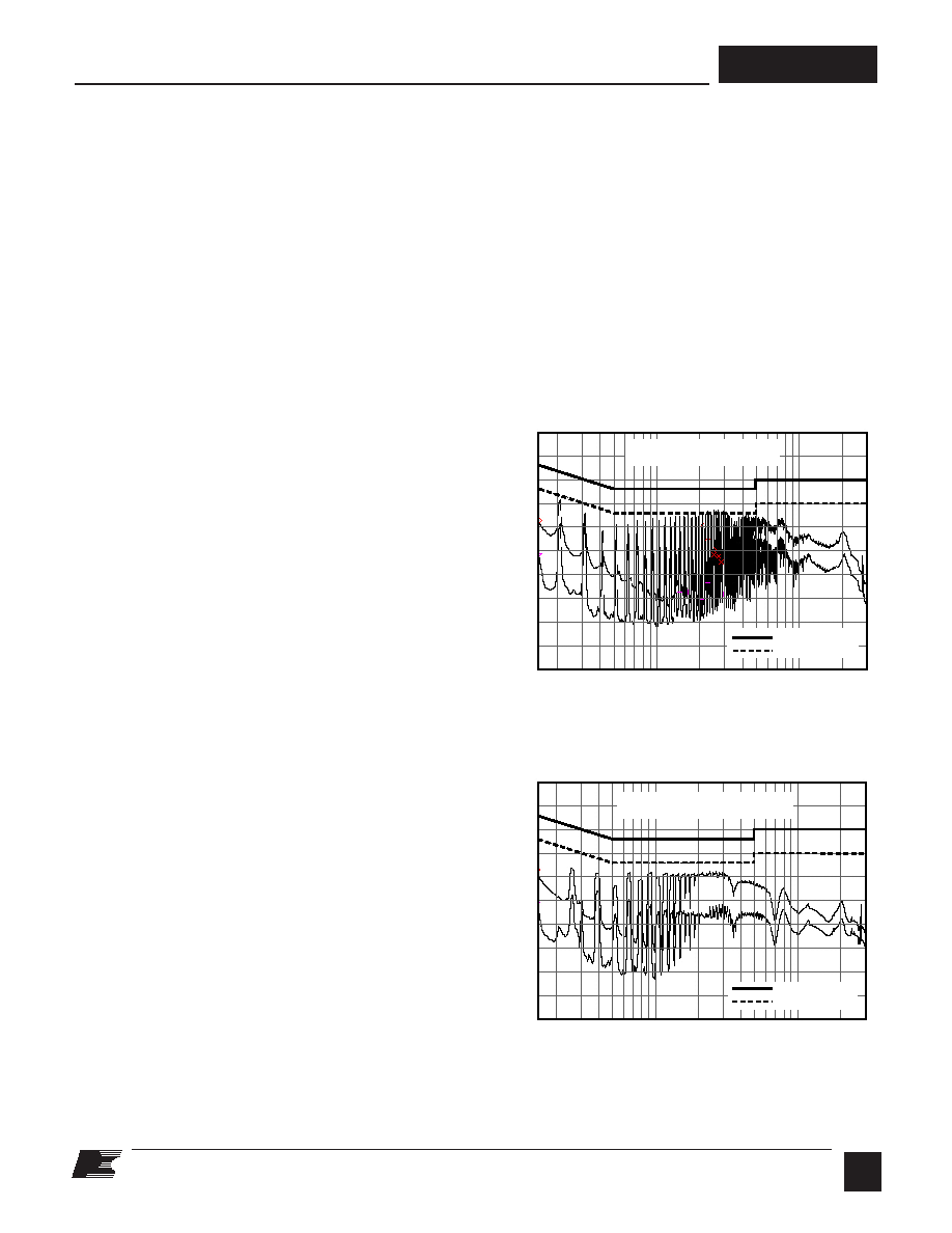
EMI
The frequency jitter feature modulates the switching frequency
over a narrow band as a means to reduce conducted EMI peaks
associated with the harmonics of the fundamental switching
frequency. This is particularly benecial for average detection
mode. As can be seen in Figure 46, the benets of jitter increase
with the order of the switching harmonic due to an increase in
frequency deviation.
The FREQUENCY pin of TOPSwitch-GX offers a switching
frequency option of 132 kHz or 66 kHz. In applications that
require heavy snubbers on the drain node for reducing high
-20
-10
0
-10
20
30
40
50
60
70
80
0.15
1
10
30
Frequency (MHz)
Amplitude
(dB
V)
PI-2576-010600
EN55022B (QP)
EN55022B (AV)
TOPSwitch-II (no jitter)
EN55022B (QP)
EN55022B (AV)
-20
-10
0
-10
20
30
40
50
60
70
80
0.15
1
10
30
Frequency (MHz)
Amplitude
(dB
V)
PI-2577-010600
TOPSwitch-GX (with jitter)
Figure 46a. TOPSwitch-II Full Range EMI Scan (100 kHz, No Jitter).
Figure 46b. TOPSwitch-GX Full Range EMI Scan (132 kHz, With
Jitter) with Identical Circuitry and Conditions.
相关PDF资料 |
PDF描述 |
|---|---|
| TOP246F | 4.32 A SWITCHING REGULATOR, 140 kHz SWITCHING FREQ-MAX, PZIP6 |
| TOP249F | 8.64 A SWITCHING REGULATOR, 140 kHz SWITCHING FREQ-MAX, PZIP6 |
| TOP244P | 2.16 A SWITCHING REGULATOR, 140 kHz SWITCHING FREQ-MAX, PDIP7 |
| TOP249FN-TL | 8.64 A SWITCHING REGULATOR, 140 kHz SWITCHING FREQ-MAX, PZIP6 |
| TOP246F-TL | 4.32 A SWITCHING REGULATOR, 140 kHz SWITCHING FREQ-MAX, PZIP6 |
相关代理商/技术参数 |
参数描述 |
|---|---|
| TOP242P | 功能描述:IC OFFLINE SWIT OVP UVLO HV 8DIP RoHS:否 类别:集成电路 (IC) >> PMIC - AC-DC 转换器,离线开关 系列:TOPSwitch®-GX 标准包装:1 系列:FPS™ 输出隔离:隔离 频率范围:61kHz ~ 73kHz 输入电压:8 V ~ 26 V 输出电压:650V 功率(瓦特):12W 工作温度:-40°C ~ 115°C 封装/外壳:8-DIP(0.300",7.62mm) 供应商设备封装:8-MDIP 包装:Digi-Reel® 其它名称:FSL206MRBNFSDKR |
| TOP242P- | 制造商:POWERINT 制造商全称:Power Integrations, Inc. 功能描述:TOPSwitch-GX Family Extended Power, Design Flexible, EcoSmart, Integrated Off-line Switcher |
| TOP242P/G | 制造商:未知厂家 制造商全称:未知厂家 功能描述:Up to 290 W Extended power. design flexible. |
| TOP242PN | 功能描述:交流/直流开关转换器 10W 85-265 VAC 15W 230 VAC RoHS:否 制造商:STMicroelectronics 输出电压:800 V 输入/电源电压(最大值):23.5 V 输入/电源电压(最小值):11.5 V 开关频率:115 kHz 电源电流:1.6 mA 工作温度范围:- 40 C to + 150 C 安装风格:SMD/SMT 封装 / 箱体:SSO-10 封装:Reel |
| TOP242PN- | 制造商:POWERINT 制造商全称:Power Integrations, Inc. 功能描述:TOPSwitch-GX Family Extended Power, Design Flexible, EcoSmart, Integrated Off-line Switcher |
发布紧急采购,3分钟左右您将得到回复。