- 您现在的位置:买卖IC网 > PDF目录68612 > TOP242G-TL (POWER INTEGRATIONS INC) 0.72 A SWITCHING REGULATOR, 140 kHz SWITCHING FREQ-MAX, PDSO7 PDF资料下载
参数资料
| 型号: | TOP242G-TL |
| 厂商: | POWER INTEGRATIONS INC |
| 元件分类: | 稳压器 |
| 英文描述: | 0.72 A SWITCHING REGULATOR, 140 kHz SWITCHING FREQ-MAX, PDSO7 |
| 封装: | PLASTIC, SMD-8/7 |
| 文件页数: | 50/52页 |
| 文件大小: | 2175K |
| 代理商: | TOP242G-TL |
第1页第2页第3页第4页第5页第6页第7页第8页第9页第10页第11页第12页第13页第14页第15页第16页第17页第18页第19页第20页第21页第22页第23页第24页第25页第26页第27页第28页第29页第30页第31页第32页第33页第34页第35页第36页第37页第38页第39页第40页第41页第42页第43页第44页第45页第46页第47页第48页第49页当前第50页第51页第52页
TOP242-250
7
N
4/05
internal capacitance between two voltage levels to create
a sawtooth waveform for the pulse width modulator. This
oscillator sets the pulse width modulator/current limit latch at
the beginning of each cycle.
The nominal switching frequency of 132 kHz was chosen to
minimize transformer size while keeping the fundamental EMI
frequency below 150 kHz. The FREQUENCY pin (available
only inY, R or F package), when shorted to the CONTROLpin,
lowerstheswitchingfrequencyto66kHz(halffrequency)which
may be preferable in some cases such as noise sensitive video
applications or a high efciency standby mode. Otherwise, the
FREQUENCY pin should be connected to the SOURCE pin
for the default 132 kHz.
To further reduce the EMI level, the switching frequency is
jittered (frequency modulated) by approximately ±4 kHz at
250 Hz (typical) rate as shown in Figure 9. Figure 46 shows
the typical improvement of EMI measurements with frequency
jitter.
Pulse Width Modulator and Maximum Duty Cycle
The pulse width modulator implements voltage mode control
by driving the output MOSFET with a duty cycle inversely
proportional to the current into the CONTROL pin that
is in excess of the internal supply current of the chip (see
Figure 7). The excess current is the feedback error signal that
appearsacrossR
E (see Figure 2). This signal is ltered by an RC
network with a typical corner frequency of 7 kHz to reduce the
effect of switching noise in the chip supply current generated
by the MOSFET gate driver. The ltered error signal is
compared with the internal oscillator sawtooth waveform to
generate the duty cycle waveform. As the control current
increases, the duty cycle decreases. A clock signal from the
oscillator sets a latch which turns on the output MOSFET. The
pulse width modulator resets the latch, turning off the output
MOSFET. Note that a minimum current must be driven into
the CONTROL pin before the duty cycle begins to change.
The maximum duty cycle, DC
MAX, is set at a default maximum
value of 78% (typical). However, by connecting the LINE-
SENSE or MULTI-FUNCTION pin (depending on the
package) to the rectied DC high voltage bus through a
resistor with appropriate value, the maximum duty cycle can
be made to decrease from 78% to 38% (typical) as shown in
Figure 11 when input line voltage increases (see line feed
forward with DC
MAX reduction).
Light Load Frequency Reduction
The pulse width modulator duty cycle reduces as the load at
the power supply output decreases. This reduction in duty
cycle is proportional to the current owing into the CONTROL
pin. As the CONTROL pin current increases, the duty cycle
decreases linearly towards a duty cycle of 10%. Below 10%
duty cycle, to maintain high efciency at light loads, the
frequency is also reduced linearly until a minimum frequency
is reached at a duty cycle of 0% (refer to Figure 7). The
minimum frequency is typically 30 kHz and 15 kHz for
132 kHz and 66 kHz operation, respectively.
This feature allows a power supply to operate at lower
frequency at light loads thus lowering the switching losses
while maintaining good cross regulation performance and low
output ripple.
Error Amplier
The shunt regulator can also perform the function of an error
amplier in primary side feedback applications. The shunt
regulator voltage is accurately derived from a temperature-
compensated bandgap reference. The gain of the error
amplier is set by the CONTROL pin dynamic impedance.
The CONTROL pin clamps external circuit signals to the V
C
voltage level. The CONTROL pin current in excess of the
supply current is separated by the shunt regulator and ows
through R
E as a voltage error signal.
On-Chip Current Limit with External Programmability
The cycle-by-cycle peak drain current limit circuit uses the
output MOSFET ON-resistance as a sense resistor. A current
limit comparator compares the output MOSFET on-state drain
to source voltage, V
DS(ON) with a threshold voltage. High drain
current causes V
DS(ON) to exceed the threshold voltage and turns
the output MOSFET off until the start of the next clock cycle.
The current limit comparator threshold voltage is temperature
compensated to minimize the variation of the current limit due
totemperaturerelatedchangesin R
DS(ON)of the output MOSFET.
The default current limit of TOPSwitch-GX is preset internally.
However, with a resistor connected between EXTERNAL
CURRENT LIMIT (X) pin (Y, R or F package) or MULTI-
FUNCTION (M) pin (P or G package) and SOURCE pin,
current limit can be programmed externally to a lower level
between 30% and 100% of the default current limit. Please
refer to the graphs in the typical performance characteristics
section for the selection of the resistor value. By setting current
limit low, a larger TOPSwitch-GX than necessary for the power
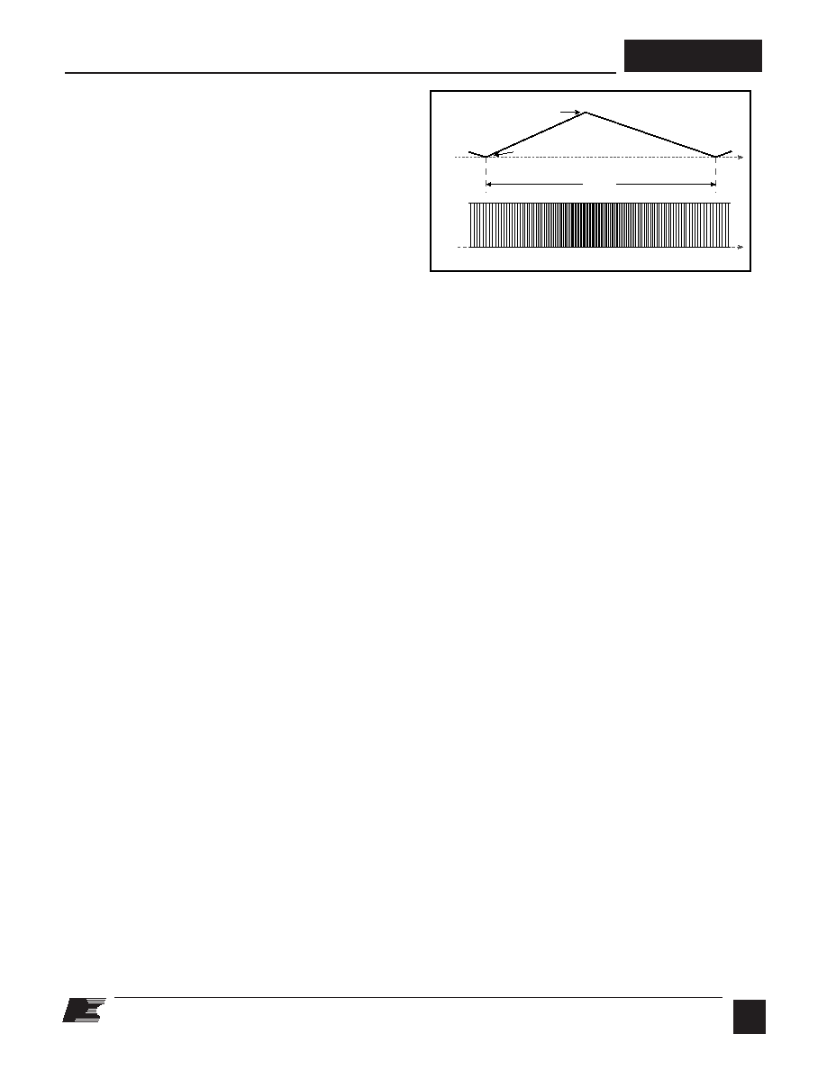
PI-2550-092499
128 kHz
4 ms
Time
Switching
Frequency
VDRAIN
136 kHz
Figure 9. Switching Frequency Jitter (Idealized V
DRAIN Waveforms).
相关PDF资料 |
PDF描述 |
|---|---|
| TOP246F | 4.32 A SWITCHING REGULATOR, 140 kHz SWITCHING FREQ-MAX, PZIP6 |
| TOP249F | 8.64 A SWITCHING REGULATOR, 140 kHz SWITCHING FREQ-MAX, PZIP6 |
| TOP244P | 2.16 A SWITCHING REGULATOR, 140 kHz SWITCHING FREQ-MAX, PDIP7 |
| TOP249FN-TL | 8.64 A SWITCHING REGULATOR, 140 kHz SWITCHING FREQ-MAX, PZIP6 |
| TOP246F-TL | 4.32 A SWITCHING REGULATOR, 140 kHz SWITCHING FREQ-MAX, PZIP6 |
相关代理商/技术参数 |
参数描述 |
|---|---|
| TOP242P | 功能描述:IC OFFLINE SWIT OVP UVLO HV 8DIP RoHS:否 类别:集成电路 (IC) >> PMIC - AC-DC 转换器,离线开关 系列:TOPSwitch®-GX 标准包装:1 系列:FPS™ 输出隔离:隔离 频率范围:61kHz ~ 73kHz 输入电压:8 V ~ 26 V 输出电压:650V 功率(瓦特):12W 工作温度:-40°C ~ 115°C 封装/外壳:8-DIP(0.300",7.62mm) 供应商设备封装:8-MDIP 包装:Digi-Reel® 其它名称:FSL206MRBNFSDKR |
| TOP242P- | 制造商:POWERINT 制造商全称:Power Integrations, Inc. 功能描述:TOPSwitch-GX Family Extended Power, Design Flexible, EcoSmart, Integrated Off-line Switcher |
| TOP242P/G | 制造商:未知厂家 制造商全称:未知厂家 功能描述:Up to 290 W Extended power. design flexible. |
| TOP242PN | 功能描述:交流/直流开关转换器 10W 85-265 VAC 15W 230 VAC RoHS:否 制造商:STMicroelectronics 输出电压:800 V 输入/电源电压(最大值):23.5 V 输入/电源电压(最小值):11.5 V 开关频率:115 kHz 电源电流:1.6 mA 工作温度范围:- 40 C to + 150 C 安装风格:SMD/SMT 封装 / 箱体:SSO-10 封装:Reel |
| TOP242PN- | 制造商:POWERINT 制造商全称:Power Integrations, Inc. 功能描述:TOPSwitch-GX Family Extended Power, Design Flexible, EcoSmart, Integrated Off-line Switcher |
发布紧急采购,3分钟左右您将得到回复。