- 您现在的位置:买卖IC网 > PDF目录19730 > TOP244GN (Power Integrations)IC OFFLINE SWIT OVP UVLO HV 8SMD PDF资料下载
参数资料
| 型号: | TOP244GN |
| 厂商: | Power Integrations |
| 文件页数: | 10/52页 |
| 文件大小: | 0K |
| 描述: | IC OFFLINE SWIT OVP UVLO HV 8SMD |
| 标准包装: | 50 |
| 系列: | TOPSwitch®-GX |
| 输出隔离: | 隔离 |
| 频率范围: | 66 ~ 132kHz |
| 输出电压: | 700V |
| 功率(瓦特): | 28W |
| 工作温度: | -40°C ~ 150°C |
| 封装/外壳: | 8-SMD(7 个接脚),鸥形翼 |
| 供应商设备封装: | SMD-8B |
| 包装: | 管件 |
第1页第2页第3页第4页第5页第6页第7页第8页第9页当前第10页第11页第12页第13页第14页第15页第16页第17页第18页第19页第20页第21页第22页第23页第24页第25页第26页第27页第28页第29页第30页第31页第32页第33页第34页第35页第36页第37页第38页第39页第40页第41页第42页第43页第44页第45页第46页第47页第48页第49页第50页第51页第52页
�� �
�
�TOP242-250�
�Bandgap� Reference�
�All� critical� TOPSwitch-GX� internal� voltages� are� derived� from�
�a� temperature-compensated� bandgap� reference.� This� reference�
�is� also� used� to� generate� a� temperature-compensated� current�
�reference,� which� is� trimmed� to� accurately� set� the� switching�
�frequency,� MOSFET� gate� drive� current,� current� limit,� and� the�
�line� OV/UV� thresholds.� TOPSwitch-GX� has� improved� circuitry�
�to� maintain� all� of� the� above� critical� parameters� within� very� tight�
�absolute� and� temperature� tolerances.�
�High-Voltage� Bias� Current� Source�
�This� current� source� biases� TOPSwitch-GX� from� the� DRAIN�
�pin� and� charges� the� CONTROL� pin� external� capacitance�
�during� start-up� or� hysteretic� operation.� Hysteretic� operation�
�occurs� during� auto-restart,� remote� OFF� and� over-temperature�
�shutdown.� In� this� mode� of� operation,� the� current� source�
�is� switched� on� and� off� with� an� effective� duty� cycle� of�
�approximately� 35%.� This� duty� cycle� is� determined� by� the�
�ratio� of� CONTROL� pin� charge� (I� C� )� and� discharge� currents�
�(I� CD1� and� I� CD2� ).� This� current� source� is� turned� off� during� normal�
�operation� when� the� output� MOSFET� is� switching.� The� effect� of�
�the� current� source� switching� will� be� seen� on� the� DRAIN� voltage�
�waveform� as� small� disturbances� and� is� normal.�
�Using� Feature� Pins�
�FREQUENCY� (F)� Pin� Operation�
�The� FREQUENCY� pin� is� a� digital� input� pin� available� in� the�
�Y,� R� or� F� package� only.� Shorting� the� FREQUENCY� pin� to�
�SOURCE� pin� selects� the� nominal� switching� frequency� of�
�132� kHz� (Figure� 13),� which� is� suited� for� most� applications.�
�For� other� cases� that� may� bene?t� from� lower� switching�
�frequency� such� as� noise� sensitive� video� applications,� a�
�66� kHz� switching� frequency� (half� frequency)� can� be� selected� by�
�shorting� the� FREQUENCY� pin� to� the� CONTROL� pin�
�(Figure� 14).� In� addition,� an� example� circuit� shown� in� Figure� 15�
�may� be� used� to� lower� the� switching� frequency� from� 132� kHz� in�
�normal� operation� to� 66� kHz� in� standby� mode� for� very� low�
�standby� power� consumption.�
�LINE-SENSE� (L)� Pin� Operation� (Y,� R� and� F� Packages)�
�When� current� is� fed� into� the� LINE-SENSE� pin,� it� works� as�
�a� voltage� source� of� approximately� 2.6� V� up� to� a� maximum�
�current� of� +400� μ� A� (typical).� At� +400� μ� A,� this� pin� turns� into�
�a� constant� current� sink.� Refer� to� Figure� 12a.� In� addition,� a�
�comparator� with� a� threshold� of� 1� V� is� connected� at� the� pin� and�
�is� used� to� detect� when� the� pin� is� shorted� to� the� SOURCE� pin.�
�There� are� a� total� of� four� functions� available� through� the� use� of�
�the� LINE-SENSE� pin:� OV,� UV,� line� feed-forward� with� DC� MAX�
�reduction,� and� remote� ON/OFF.� Connecting� the� LINE-SENSE�
�pin� to� the� SOURCE� pin� disables� all� four� functions.� The� LINE-�
�SENSE� pin� is� typically� used� for� line� sensing� by� connecting� a�
�resistor� from� this� pin� to� the� recti?ed� DC� high� voltage� bus� to�
�implement� OV,� UV� and� DC� MAX� reduction� with� line� voltage.� In�
�this� mode,� the� value� of� the� resistor� determines� the� line� OV/UV�
�thresholds,� and� the� DC� MAX� is� reduced� linearly� with� recti?ed� DC�
�high� voltage� starting� from� just� above� the� UV� threshold.� The� pin�
�can� also� be� used� as� a� remote� ON/OFF� and� a� synchronization�
�input.� Refer� to� Table� 2� for� possible� combinations� of� the� functions�
�with� example� circuits� shown� in� Figure� 16� through� Figure� 40.� A�
�description� of� speci?c� functions� in� terms� of� the� LINE-SENSE�
�pin� I/V� characteristic� is� shown� in� Figure� 11� (right� hand� side).�
�The� horizontal� axis� represents� LINE-SENSE� pin� current� with�
�positive� polarity� indicating� currents� ?owing� into� the� pin.� The�
�meaning� of� the� vertical� axes� varies� with� functions.� For� those�
�that� control� the� ON/OFF� states� of� the� output� such� as� UV,� OV�
�and� remote� ON/OFF,� the� vertical� axis� represents� the� enable/�
�disable� states� of� the� output.� UV� triggers� at� I� UV� (+50� μ� A� typical�
�with� 30� μ� A� hysteresis)� and� OV� triggers� at� I� OV� (+225� μ� A�
�typical� with� 8� μ� A� hysteresis).� Between� the� UV� and� OV�
�thresholds,� the� output� is� enabled.� For� line� feed-forward� with�
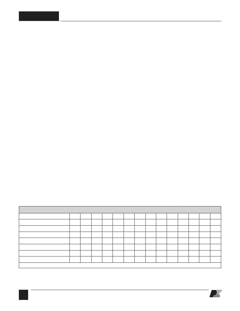
�LINE-SENSE� AND� EXTERNAL� CURRENT� LIMIT� PIN� TABLE*�
�Figure� Number�
�16�
�17�
�18�
�19�
�20�
�21�
�22�
�23�
�24�
�25�
�26�
�27�
�28�
�29�
�Three� Terminal� Operation�
�?�
�Under-Voltage�
�Overvoltage�
�Line� Feed-Forward� (DC� MAX� )�
�Overload� Power� Limiting�
�?�
�?�
�?�
�?�
�?�
�?�
�?�
�?�
�?�
�?�
�?�
�?�
�?�
�?�
�?�
�External� Current� Limit�
�?�
�?�
�?�
�?�
�?�
�?�
�Remote� ON/OFF�
�?�
�?�
�?�
�?�
�?�
�?�
�?�
�*This� table� is� only� a� partial� list� of� many� LINE-SENSE� and� EXTERNAL� CURRENT� LIMIT� pin� con?gurations� that� are� possible.�
�Table� 2.� Typical� LINE-SENSE� and� EXTERNAL� CURRENT� LIMIT� Pin� Con?gurations.�
�10�
�O�
�11/05�
�相关PDF资料 |
PDF描述 |
|---|---|
| MIC2586-2BM TR | IC CTRLR/SEQ HOT SWAP 14-SOIC |
| VE-24L-CY-F2 | CONVERTER MOD DC/DC 28V 50W |
| MIC2586-1BM TR | IC CTRLR/SEQ HOT SWAP 14-SOIC |
| MIC37150-3.3BR | IC REG LDO 3.3V 1.5A S-PAK-3 |
| VE-242-CY-F1 | CONVERTER MOD DC/DC 15V 50W |
相关代理商/技术参数 |
参数描述 |
|---|---|
| TOP244GN- | 制造商:POWERINT 制造商全称:Power Integrations, Inc. 功能描述:TOPSwitch-GX Family Extended Power, Design Flexible, EcoSmart, Integrated Off-line Switcher |
| TOP244GN-TL | 功能描述:交流/直流开关转换器 20 W 85-265 VAC 28 W 230 VAC RoHS:否 制造商:STMicroelectronics 输出电压:800 V 输入/电源电压(最大值):23.5 V 输入/电源电压(最小值):11.5 V 开关频率:115 kHz 电源电流:1.6 mA 工作温度范围:- 40 C to + 150 C 安装风格:SMD/SMT 封装 / 箱体:SSO-10 封装:Reel |
| TOP244G-TL | 功能描述:IC OFFLINE SWIT OVP UVLO HV 8SMD RoHS:否 类别:集成电路 (IC) >> PMIC - AC-DC 转换器,离线开关 系列:TOPSwitch®-GX 标准包装:1 系列:FPS™ 输出隔离:隔离 频率范围:61kHz ~ 73kHz 输入电压:8 V ~ 26 V 输出电压:650V 功率(瓦特):12W 工作温度:-40°C ~ 115°C 封装/外壳:8-DIP(0.300",7.62mm) 供应商设备封装:8-MDIP 包装:Digi-Reel® 其它名称:FSL206MRBNFSDKR |
| TOP244P | 功能描述:IC OFFLINE SWIT OVP UVLO HV 8DIP RoHS:否 类别:集成电路 (IC) >> PMIC - AC-DC 转换器,离线开关 系列:TOPSwitch®-GX 标准包装:1 系列:FPS™ 输出隔离:隔离 频率范围:61kHz ~ 73kHz 输入电压:8 V ~ 26 V 输出电压:650V 功率(瓦特):12W 工作温度:-40°C ~ 115°C 封装/外壳:8-DIP(0.300",7.62mm) 供应商设备封装:8-MDIP 包装:Digi-Reel® 其它名称:FSL206MRBNFSDKR |
| TOP244P- | 制造商:POWERINT 制造商全称:Power Integrations, Inc. 功能描述:TOPSwitch-GX Family Extended Power, Design Flexible, EcoSmart, Integrated Off-line Switcher |
发布紧急采购,3分钟左右您将得到回复。