- 您现在的位置:买卖IC网 > PDF目录19891 > TOP257MG (Power Integrations)IC OFFLINE SWIT PROG OVP 10CSDIP PDF资料下载
参数资料
| 型号: | TOP257MG |
| 厂商: | Power Integrations |
| 文件页数: | 12/50页 |
| 文件大小: | 0K |
| 描述: | IC OFFLINE SWIT PROG OVP 10CSDIP |
| 标准包装: | 50 |
| 输出隔离: | 隔离 |
| 频率范围: | 59.4kHz ~ 72.6kHz |
| 输出电压: | 700V |
| 功率(瓦特): | 41W |
| 工作温度: | -40°C ~ 150°C |
| 封装/外壳: | 10-SDIP(0.300",7.62mm),9 引线 |
| 供应商设备封装: | SDIP-10C |
| 包装: | 管件 |
| 其它名称: | 596-1334-5 |
第1页第2页第3页第4页第5页第6页第7页第8页第9页第10页第11页当前第12页第13页第14页第15页第16页第17页第18页第19页第20页第21页第22页第23页第24页第25页第26页第27页第28页第29页第30页第31页第32页第33页第34页第35页第36页第37页第38页第39页第40页第41页第42页第43页第44页第45页第46页第47页第48页第49页第50页
�� �
�
�TOP252-262�
�M� Pin�
�X� Pin�
�V� Pin�
�I� REM(N)�
�I� UV�
�I� OV�
�I� OV(LS)�
�(Enabled)�
�Output�
�MOSFET�
�Switching�
�(Disabled)�
�Disabled� when� supply�
�output� goes� out� of�
�regulation�
�(Non-Latching)�
�(Latching)�
�I�
�I� LIMIT� (Default)�
�Current�
�Limit�
�I�
�DC� MAX� (78%)�
�Maximum�
�Duty� Cycle�
�I�
�V� BG�
�Pin� Voltage�
�-250�
�-200�
�-150�
�-100�
�-50�
�0�
�25�
�50�
�75�
�100�
�125�
�336�
�I�
�X� and� V� Pins� (Y,� E,� L� and� M� Packages)� and� M� Pin� (P� and� G� Packages)� Current� (� μ� A)�
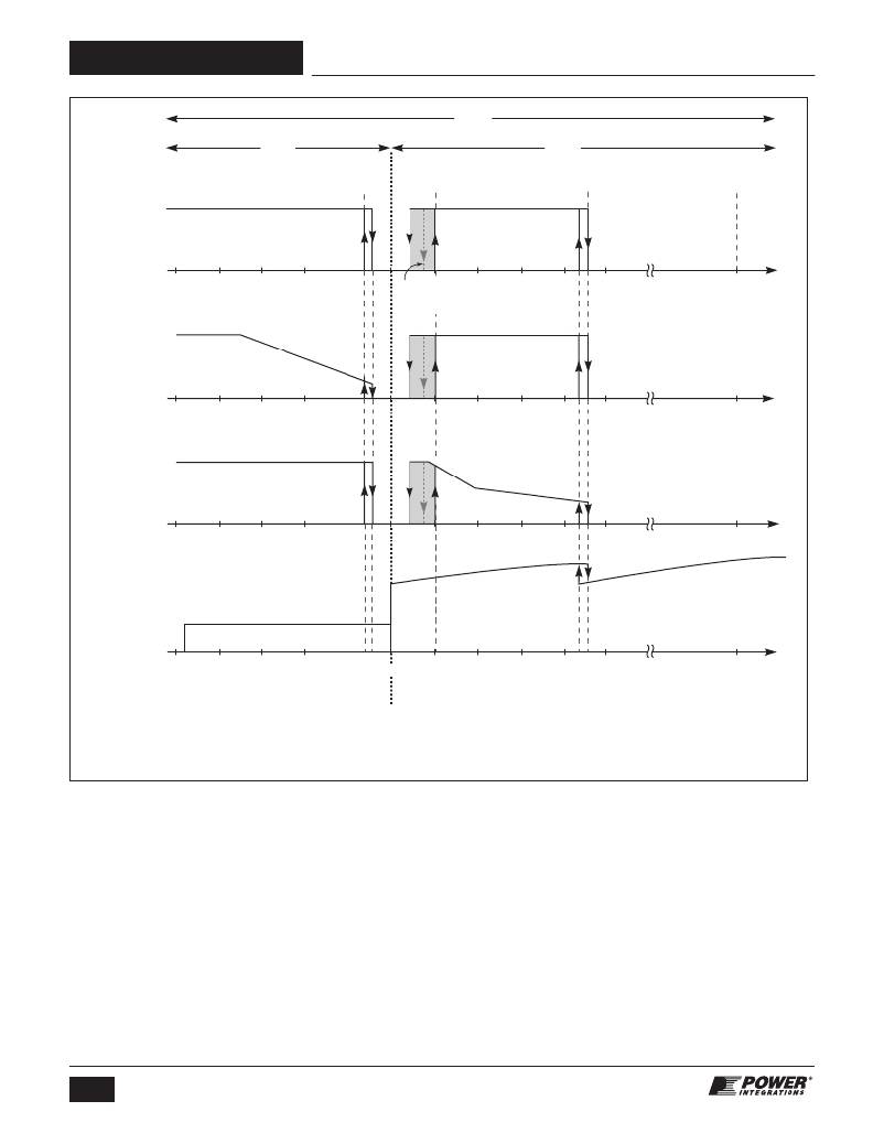
�Note:� This� figure� provides� idealized� functional� characteristics� with� typical� performance� values.� Please� refer� to� the� parametric�
�table� and� typical� performance� characteristics� sections� of� the� data� sheet� for� measured� data.� For� a� detailed� description� of�
�each� functional� pin� operation� refer� to� the� Functional� Description� section� of� the� data� sheet.�
�PI-4646-071708�
�Figure� 12.� MULTI-FUNCTION� (P� and� G� package).� VOLTAGE� MONITOR� and� EXTERNAL� CURRENT� LIMIT� (Y,� E/L� and� M� package)� Pin� Characteristics.�
�The� circuit� examples� shown� in� Figures� 41,� 42� and� 43� show� a�
�simple� method� for� implementing� the� primary� sensed� over-�
�voltage� protection.�
�During� a� fault� condition� resulting� from� loss� of� feedback,� output�
�voltage� will� rapidly� rise� above� the� nominal� voltage.� The� increase�
�in� output� voltage� will� also� result� in� an� increase� in� the� voltage� at�
�the� output� of� the� bias� winding.� A� voltage� at� the� output� of� the�
�bias� winding� that� exceeds� of� the� sum� of� the� voltage� rating� of� the�
�Zener� diode� connected� from� the� bias� winding� output� to� the�
�V-pin� (or� M-pin)� and� V-pin� (or� M-pin)� voltage,� will� cause� a� current�
�in� excess� of� I� V� or� I� M� to� be� injected� into� the� V-pin�
�(or� M-pin),� which� will� trigger� the� OVP� feature.�
�The� primary� sensed� OVP� protection� circuit� shown� in� Figures� 41,�
�42� and� 43� is� triggered� by� a� significant� rise� in� output� voltage� (and�
�therefore� bias� winding� voltage).� If� the� power� supply� is� operating�
�under� heavy� load� or� low� input� line� conditions� when� an� open�
�loop� occurs,� the� output� voltage� may� not� rise� significantly.�
�Under� these� conditions,� a� latching� shutdown� will� not� occur� until�
�load� or� line� conditions� change.� Nevertheless,� the� operation�
�provides� the� desired� protection� by� preventing� significant� rise� in�
�the� output� voltage� when� the� line� or� load� conditions� do� change.�
�Primary� side� OVP� protection� with� the� TOPSwitch-HX� in� a� typical�
�application� will� prevent� a� nominal� 12� V� output� from� rising� above�
�approximately� 20� V� under� open� loop� conditions.� If� greater�
�accuracy� is� required,� a� secondary� sensed� OVP� circuit� is�
�recommended.�
�12�
�Rev.� H� 06/13�
�www.powerint.com�
�相关PDF资料 |
PDF描述 |
|---|---|
| VI-B1V-CY-F1 | CONVERTER MOD DC/DC 5.8V 50W |
| TOP267VG | IC OFFLINE SW PWM OCP OVP 12EDIP |
| T97R106M075ESA | CAP TANT 10UF 75V 20% 3024 |
| GRM2165C1H751JA01D | CAP CER 750PF 50V 5% NP0 0805 |
| AT17N256-10PI | IC FPGA 256K CONFIG MEM 8DIP |
相关代理商/技术参数 |
参数描述 |
|---|---|
| TOP257MN | 功能描述:交流/直流开关转换器 Off-Line Switcher IC 30W/78W PK RoHS:否 制造商:STMicroelectronics 输出电压:800 V 输入/电源电压(最大值):23.5 V 输入/电源电压(最小值):11.5 V 开关频率:115 kHz 电源电流:1.6 mA 工作温度范围:- 40 C to + 150 C 安装风格:SMD/SMT 封装 / 箱体:SSO-10 封装:Reel |
| TOP257PG | 功能描述:交流/直流开关转换器 30W/45W PK 85-264VAC 41W/70W PK (230V AC) RoHS:否 制造商:STMicroelectronics 输出电压:800 V 输入/电源电压(最大值):23.5 V 输入/电源电压(最小值):11.5 V 开关频率:115 kHz 电源电流:1.6 mA 工作温度范围:- 40 C to + 150 C 安装风格:SMD/SMT 封装 / 箱体:SSO-10 封装:Reel |
| TOP257PN | 功能描述:交流/直流开关转换器 Off-Line Switcher IC 30W/45W PK RoHS:否 制造商:STMicroelectronics 输出电压:800 V 输入/电源电压(最大值):23.5 V 输入/电源电压(最小值):11.5 V 开关频率:115 kHz 电源电流:1.6 mA 工作温度范围:- 40 C to + 150 C 安装风格:SMD/SMT 封装 / 箱体:SSO-10 封装:Reel |
| TOP257YN | 功能描述:交流/直流开关转换器 Off-Line Switcher IC 119W RoHS:否 制造商:STMicroelectronics 输出电压:800 V 输入/电源电压(最大值):23.5 V 输入/电源电压(最小值):11.5 V 开关频率:115 kHz 电源电流:1.6 mA 工作温度范围:- 40 C to + 150 C 安装风格:SMD/SMT 封装 / 箱体:SSO-10 封装:Reel |
| TOP258EG | 功能描述:交流/直流开关转换器 148W (85-264VAC) 195W (230V AC) RoHS:否 制造商:STMicroelectronics 输出电压:800 V 输入/电源电压(最大值):23.5 V 输入/电源电压(最小值):11.5 V 开关频率:115 kHz 电源电流:1.6 mA 工作温度范围:- 40 C to + 150 C 安装风格:SMD/SMT 封装 / 箱体:SSO-10 封装:Reel |
发布紧急采购,3分钟左右您将得到回复。