- 您现在的位置:买卖IC网 > PDF目录22107 > TOP269EG (Power Integrations)IC OFFLINE SW PWM OCP OVP 7ESIP PDF资料下载
参数资料
| 型号: | TOP269EG |
| 厂商: | Power Integrations |
| 文件页数: | 15/40页 |
| 文件大小: | 0K |
| 描述: | IC OFFLINE SW PWM OCP OVP 7ESIP |
| 特色产品: | TopSwitch?-JX Integrated Switcher Ics |
| 标准包装: | 48 |
| 输出隔离: | 隔离 |
| 频率范围: | 66 ~ 132kHz |
| 输出电压: | 725V |
| 功率(瓦特): | 120W |
| 工作温度: | -40°C ~ 150°C |
| 封装/外壳: | 7-SIP,6 引线,裸露焊盘,成形引线 |
| 供应商设备封装: | eSIP-7C |
| 包装: | 管件 |
| 其它名称: | 596-1278-5 |
第1页第2页第3页第4页第5页第6页第7页第8页第9页第10页第11页第12页第13页第14页当前第15页第16页第17页第18页第19页第20页第21页第22页第23页第24页第25页第26页第27页第28页第29页第30页第31页第32页第33页第34页第35页第36页第37页第38页第39页第40页
�� �
�
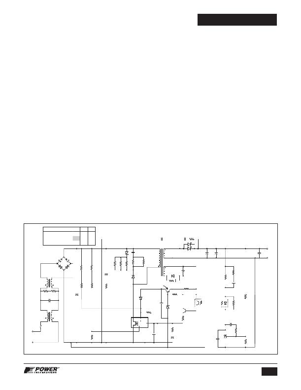
�TOP264-271�
�Application� Example�
�Low� No-Load,� High� Efficiency,� 65� W,� Universal� Input�
�Adapter� Power� Supply�
�The� circuit� shown� in� Figure� 25� shows� a� 90� VAC� to� 265� VAC�
�input,� 19� V,� 3.42� A� output� power� supply,� designed� for� operation�
�inside� a� sealed� adapter� case� type.� The� goals� of� the� design� were�
�highest� full� load� efficiency,� highest� average� efficiency� (average� of�
�25%,� 50%,� 75%� and� 100%� load� points),� and� very� low� no-load�
�consumption.� Additional� requirements� included� latching� output�
�overvoltage� shutdown� and� compliance� to� safety� agency� limited�
�power� source� (LPS)� limits.� Measured� efficiency� and� no-load�
�performance� is� summarized� in� the� table� shown� in� the� schematic�
�which� easily� exceed� current� energy� efficiency� requirements.�
�In� order� to� meet� these� design� goals� the� following� key� design�
�decisions� were� made.�
�PI� Part� Selection�
�? � One� device� size� larger� selected� than� required� for� power�
�delivery� to� increase� efficiency�
�The� current� limit� programming� feature� of� TOPSwitch-JX� allows�
�the� selection� of� a� larger� device� than� needed� for� power� delivery.�
�This� gives� higher� full� load,� low-line� efficiency� by� reducing� the�
�MOSFET� conduction� losses� (I� RMS2� � R� DS(ON)� )� but� maintains� the�
�overload� power,� transformer� and� other� components� size� as� if� a�
�smaller� device� had� been� used.�
�For� this� design� one� device� size� larger� than� required� for� power�
�delivery� (as� recommended� by� the� power� table)� was� selected.�
�This� typically� gives� the� highest� efficiency.� Further� increases� in�
�device� size� often� results� in� the� same� or� lower� efficiency� due� to�
�the� larger� switching� losses� associated� with� a� larger� MOSFET.�
�Line� Sense� Resistor� Values�
�? � Increasing� line� sensing� resistance� from� 4� M� W� to� 10.2� M� W� to�
�reduce� no-load� input� power� dissipation� by� 16� mW�
�Line� sensing� is� provided� by� resistors� R3� and� R4� and� sets� the�
�line� undervoltage� and� overvoltage� thresholds.� The� combined�
�value� of� these� resistors� was� increased� from� the� standard� 4� M� W�
�to� 10.2� M� W� .� This� reduced� the� resistor� dissipation,� and� therefore�
�contribution� to� no-load� input� power,� from� ~26� mW� to� ~10� mW.� To�
�compensate� the� resultant� change� in� the� UV� (turn-on)� threshold�
�resistor� R20� was� added� between� the� CONTROL� and� VOLTAGE-�
�MONITOR� pins.� This� adds� a� DC� current� equal� to� ~16� m� A� into� the�
�V� pin,� requiring� only� 9� m� A� to� be� provided� via� R3� and� R4� to� reach�
�the� V� pin� UV� (turn-on)� threshold� current� of� 25� m� A� and� setting� the�
�UV� threshold� to� 95� VDC.�
�This� technique� does� effectively� disable� the� line� OV� feature� as�
�the� resultant� OV� threshold� is� raised� from� ~450� VDC� to� ~980� VDC.�
�However� in� this� design� there� was� no� impact� as� the� value� of�
�input� capacitance� (C2)� was� sufficient� to� allow� the� design� to�
�withstand� differential� line� surges� greater� than� 2� kV� without� the�
�peak� drain� voltage� reaching� the� BV� DSS� rating� of� U1.�
�Specific� guidelines� and� detailed� calculations� for� the� value� of�
�R20� may� be� found� in� the� TOPSwitch-JX� Application� Note� (AN-47).�
�Clamp� Configuration� –� RZCD� vs� RCD�
�? � An� RZCD� (Zener� bleed)� was� selected� over� an� RCD� clamp� to�
�give� higher� light� load� efficiency� and� lower� no-load� consumption�
�The� clamp� network� is� formed� by� VR2,� C4,� R5,� R6,� R11,� R28,�
�R29� and� D2.� It� limits� the� peak� drain� voltage� spike� caused� by�
�leakage� inductance� to� below� the� BV� DSS� rating� of� the� internal�
�Input� Voltage� (VAC)�
�Full� Power� Ef?ciency� (%)�
�Average� Ef?ciency� (%)�
�90�
�86.6�
�115�
�88.4�
�89.8�
�230�
�89.1�
�89.5�
�C11�
�1� nF�
�250� VAC�
�C12�
�1� nF� R15�
�100� V� 33� ?�
�No-load� Input� Power� (mW)�
�57.7�
�59.7�
�86.7�
�VR2�
�SMAJ250A�
�T1�
�3� RM10� FL1�
�C13� C14�
�470� μ� F� 470� μ� F�
�25� V� 25� V�
�19� V,� 3.42� A�
�R29�
�300� ?�
�4�
�R14�
�20� ?�
�4.7� k� ?�
�R25�
�L�
�N�
�D1�
�GBU8J�
�600� V�
�L3�
�12� mH�
�R1� R2�
�2.2� M� ?� 2.2� M� ?�
�C1�
�330� nF�
�275� VAC�
�L4�
�200� μ� H�
�F1�
�4A�
�90� -� 265�
�VAC�
�C2�
�120� μ� F�
�400� V�
�R3�
�5.1� M� ?�
�R4�
�5.1� M� ?�
�R9�
�11� k� ?�
�1%�
�R7�
�10� M� ?�
�R8�
�10� M� ?�
�R5�
�300� ?�
�R11�
�300� ?�
�C5�
�2.2� nF�
�1� kV�
�R24�
�2.2� ?�
�TOPSwitch-JX�
�U1�
�TOP269EG�
�D�
�S�
�C4�
�1000� pF�
�630� V�
�R6� R28�
�150� ?� 300� ?�
�1�
�D2�
�RS1K�
�Q1�
�MMBT4403�
�D3�
�BAV19WS�
�C9�
�220� nF�
�25� V�
�R20�
�191� k� ?�
�1%�
�V�
�CONTROL�
�C�
�X� F�
�C6�
�100� nF�
�50� V�
�D5�
�V30100C�
�FL2�
�5�
�D4� C10�
�BAV21WS-� 56� μ� F�
�7-F� 35� V�
�C15�
�470� pF�
�50� V�
�R10�
�100� ?�
�R12�
�U3B�
�PS2501-�
�1-H-A�
�VR1�
�ZMM5244B-7�
�Q2�
�MMBT3904�
�20� ?�
�1/8� W�
�R13�
�6.8� ?�
�1/8� W�
�C7�
�47� μ� F�
�16� V�
�R16�
�20� k� ?�
�U3A�
�PS2501-�
�1-H-A�
�C22�
�100� nF�
�50� V�
�R22�
�1.6� k� ?�
�C19�
�6.8� nF�
�50� V�
�R17�
�147� k� ?�
�1%�
�R27�
�10� k� ?�
�C16�
�22� nF�
�50� V�
�R19�
�20� k� ?�
�U2�
�LMV431AIMF�
�1%�
�C21�
�10� nF�
�50� V�
�R18�
�10� k� ?�
�1%�
�RTN�
�PI-5667-030810�
�Figure� 25.� Schematic� of� High� Efficiency� 19� V,� 65� W,� Universal� Input� Flyback� Supply� With� Low� No-load.�
�15�
�www.powerint.com�
�Rev.� E� 08/12�
�相关PDF资料 |
PDF描述 |
|---|---|
| RMA32DTMI | CONN EDGECARD 64POS R/A .125 SLD |
| 8-530666-2 | CONN LOW PRO 28POS .156 SOLDER |
| RSA32DTBI | CONN EDGECARD 64POS R/A .125 SLD |
| VI-232-EV-F1 | CONVERTER MOD DC/DC 15V 150W |
| R-78HB24-0.3 | CONV DC/DC 0.3A 24V OUT SIP VERT |
相关代理商/技术参数 |
参数描述 |
|---|---|
| TOP269EG/VG | 制造商:POWERINT 制造商全称:Power Integrations, Inc. 功能描述:Integrated Off-Line Switcher with EcoSmart Technology for Highly Efficient Power Supplies |
| TOP269EG-TL | 制造商:POWERINT 制造商全称:Power Integrations, Inc. 功能描述:Integrated Off-Line Switcher with EcoSmart Technology for Highly Efficient Power Supplies |
| TOP269KG | 功能描述:交流/直流开关转换器 Int Off-Line Switchr EcoSmart,55W/81W RoHS:否 制造商:STMicroelectronics 输出电压:800 V 输入/电源电压(最大值):23.5 V 输入/电源电压(最小值):11.5 V 开关频率:115 kHz 电源电流:1.6 mA 工作温度范围:- 40 C to + 150 C 安装风格:SMD/SMT 封装 / 箱体:SSO-10 封装:Reel |
| TOP269KG-TL | 功能描述:交流/直流开关转换器 Int Off-Line Switchr EcoSmart,55W/81W RoHS:否 制造商:STMicroelectronics 输出电压:800 V 输入/电源电压(最大值):23.5 V 输入/电源电压(最小值):11.5 V 开关频率:115 kHz 电源电流:1.6 mA 工作温度范围:- 40 C to + 150 C 安装风格:SMD/SMT 封装 / 箱体:SSO-10 封装:Reel |
| TOP269VG | 功能描述:交流/直流开关转换器 Int Off-Line Switchr 120W/162W RoHS:否 制造商:STMicroelectronics 输出电压:800 V 输入/电源电压(最大值):23.5 V 输入/电源电压(最小值):11.5 V 开关频率:115 kHz 电源电流:1.6 mA 工作温度范围:- 40 C to + 150 C 安装风格:SMD/SMT 封装 / 箱体:SSO-10 封装:Reel |
发布紧急采购,3分钟左右您将得到回复。