- 您现在的位置:买卖IC网 > PDF目录98270 > TPA2010D1YEFT (TEXAS INSTRUMENTS INC) 2.5 W, 2 CHANNEL, AUDIO AMPLIFIER, PBGA9 PDF资料下载
参数资料
| 型号: | TPA2010D1YEFT |
| 厂商: | TEXAS INSTRUMENTS INC |
| 元件分类: | 音频/视频放大 |
| 英文描述: | 2.5 W, 2 CHANNEL, AUDIO AMPLIFIER, PBGA9 |
| 封装: | 1.45 X 1.45 MM, DSBGA-9 |
| 文件页数: | 7/25页 |
| 文件大小: | 783K |
| 代理商: | TPA2010D1YEFT |
www.ti.com
Component Location
Trace Width
SLOS417C – OCTOBER 2003 – REVISED SEPTEMBER 2007
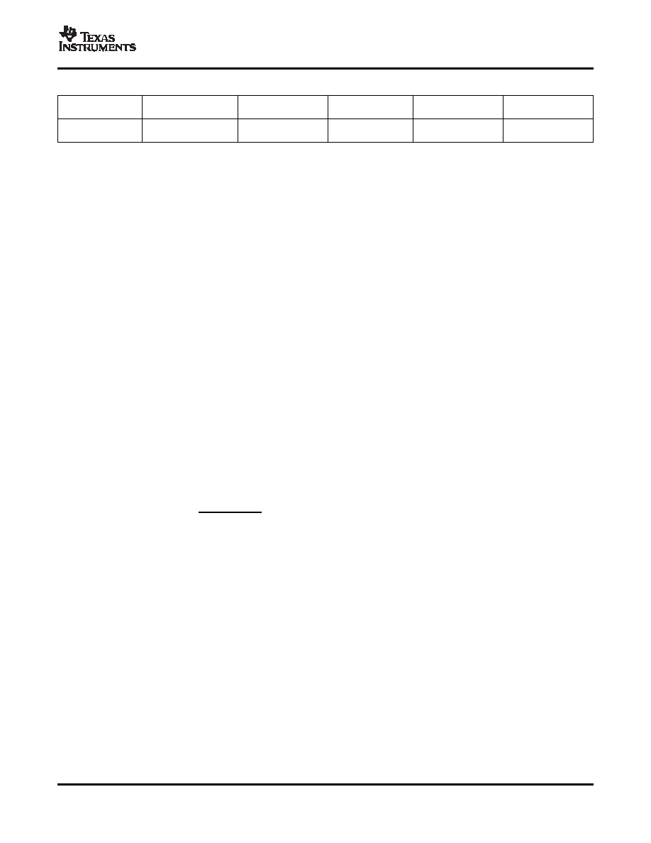
Table 2. Land Pattern Dimensions
SOLDER PAD
SOLDER MASK
COPPER
STENCIL
COPPER PAD
DEFINITIONS
OPENING
THICKNESS
OPENING
THICKNESS
Nonsolder mask
275
μm
375
μm
1 oz max (32
μm)
275
μm x 275 μm Sq.
125
μm thick
defined (NSMD)
(+0.0, –25
μm)
(+0.0, –25
μm)
(rounded corners)
NOTES:
1. Circuit traces from NSMD defined PWB lands should be 75
μm to 100 μm wide in the exposed area inside
the solder mask opening. Wider trace widths reduce device stand off and impact reliability.
2. Recommend solder paste is Type 3 or Type 4.
3. Best reilability results are achieved when the PWB laminate glass transition temperature is above the
operating the range of the intended application.
4. For a PWB using a Ni/Au surface finish, the gold thickness should be less 0.5
μm to avoid a reduction in
thermal fatigue performance.
5. Solder mask thickness should be less than 20
μm on top of the copper circuit pattern.
6. Best solder stencil preformance is achieved using laser cut stencils with electro polishing. Use of chemically
etched stencils results in inferior solder paste volume control.
7. Trace routing away from WCSP device should be balanced in X and Y directions to avoid unintentional
component movement due to solder wetting forces.
Place all the external components very close to the TPA2010D1. The input resistors need to be very close to the
TPA2010D1 input pins so noise does not couple on the high impedance nodes between the input resistors and
the input amplifier of the TPA2010D1. Placing the decoupling capacitor, CS, close to the TPA2010D1 is
important for the efficiency of the class-D amplifier. Any resistance or inductance in the trace between the device
and the capacitor can cause a loss in efficiency.
Recommended trace width at the solder balls is 75
μm to 100 μm to prevent solder wicking onto wider PCB
traces. Figure 34 shows the layout of the TPA2010D1 evaluation module (EVM).
For high current pins (VDD, GND VO+, and VO–) of the TPA2010D1, use 100-μm trace widths at the solder balls
and at least 500-
μm PCB traces to ensure proper performance and output power for the device.
For input pins (IN–, IN+, and SHUTDOWN) of the TPA2010D1, use 75-
μm to 100-μm trace widths at the solder
balls. IN– and IN+ pins need to run side-by-side to maximize common-mode noise cancellation. Placing input
resistors, RIN, as close to the TPA2010D1 as possible is recommended.
Copyright 2003–2007, Texas Instruments Incorporated
15
Product Folder Link(s): TPA2010D1
相关PDF资料 |
PDF描述 |
|---|---|
| TPA2010D1YZFR | 2.5 W, 2 CHANNEL, AUDIO AMPLIFIER, PBGA9 |
| TPA2010D1YZFT | 2.5 W, 2 CHANNEL, AUDIO AMPLIFIER, PBGA9 |
| TPA2010D1YEF | 2.5 W, 1 CHANNEL, AUDIO AMPLIFIER, BGA9 |
| TPA2010D1YZF | 2.5 W, 1 CHANNEL, AUDIO AMPLIFIER, BGA9 |
| TPA2011D1YFFR | 3.24 W, 1 CHANNEL, AUDIO AMPLIFIER, BGA9 |
相关代理商/技术参数 |
参数描述 |
|---|---|
| TPA2010D1YZF | 制造商:TI 制造商全称:Texas Instruments 功能描述:2.5-W MONO FILTER-FREE CLASS-D AUDIO POWER AMPLIFIER |
| TPA2010D1YZFR | 功能描述:音频放大器 Mono Filter-Free Class-D in WCSP RoHS:否 制造商:STMicroelectronics 产品:General Purpose Audio Amplifiers 输出类型:Digital 输出功率: THD + 噪声: 工作电源电压:3.3 V 电源电流: 最大功率耗散: 最大工作温度: 安装风格:SMD/SMT 封装 / 箱体:TQFP-64 封装:Reel |
| TPA2010D1YZFRG4 | 制造商:TI 功能描述:AUDIO POWER AMPLIFIER |
| TPA2010D1YZFT | 功能描述:音频放大器 Mono Filter-Free Class-D in WCSP RoHS:否 制造商:STMicroelectronics 产品:General Purpose Audio Amplifiers 输出类型:Digital 输出功率: THD + 噪声: 工作电源电压:3.3 V 电源电流: 最大功率耗散: 最大工作温度: 安装风格:SMD/SMT 封装 / 箱体:TQFP-64 封装:Reel |
| TPA2011D1 | 制造商:TI 制造商全称:Texas Instruments 功能描述:3.2W Mono Filter-Free Class-D Audio Power Amplifier With Auto-Recovering Short-Circuit Protection |
发布紧急采购,3分钟左右您将得到回复。