- 您现在的位置:买卖IC网 > PDF目录98274 > TPA5051RSATG4 (TEXAS INSTRUMENTS INC) SPECIALTY CONSUMER CIRCUIT, PQCC16 PDF资料下载
参数资料
| 型号: | TPA5051RSATG4 |
| 厂商: | TEXAS INSTRUMENTS INC |
| 元件分类: | 消费家电 |
| 英文描述: | SPECIALTY CONSUMER CIRCUIT, PQCC16 |
| 封装: | 4 X 4 MM, GREEN, PLASTIC, QFN-16 |
| 文件页数: | 21/23页 |
| 文件大小: | 812K |
| 代理商: | TPA5051RSATG4 |
www.ti.com
GENERAL I2C OPERATION
Register(N)
8-BitDatafor
Register(N+1)
SINGLE-AND MULTIPLE-BYTE TRANSFERS
SLOS497A – JUNE 2006 – REVISED JULY 2006
APPLICATION INFORMATION (continued)
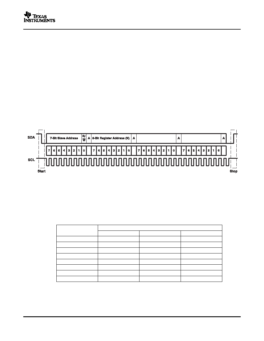
The I2C bus employs two signals; SDA (data) and SCL (clock), to communicate between integrated circuits in a
system. Data is transferred on the bus serially, one bit at a time. The address and data are transferred in byte
(8-bit) format with the most-significant bit (MSB) transferred first. In addition, each byte transferred on the bus is
acknowledged by the receiving device with an acknowledge bit. Each transfer operation begins with the master
device driving a start condition on the bus and ends with the master device driving a stop condition on the bus.
The bus uses transitions on the data terminal (SDA) while the clock is high to indicate start and stop conditions.
A high-to-low transition on SDA indicates a start and a low-to-high transition indicates a stop. Normal data-bit
transitions must occur within the low time of the clock period. These conditions are shown in Figure 5. The
master generates the 7-bit slave address and the read/write (R/W) bit to open communication with another
device and then wait for an acknowledge condition. The TPA5051 holds SDA low during acknowledge clock
period to indicate an acknowledgement. When this occurs, the master transmits the next byte of the sequence.
Each device is addressed by a unique 7-bit slave address plus R/W bit (1 byte). All compatible devices share
the same signals via a bidirectional bus using a wired-AND connection.
An external pull-up resistor must be used for the SDA and SCL signals to set the HIGH level for the bus. When
the bus level is 5 V, pull-up resistors between 1 k
and 2 k in value must be used. For a bus level of 3.3 V,
higher resistor values, such as 10 k
, may be used.
Figure 5. Typical I2C Sequence
There is no limit on the number of bytes that can be transmitted between start and stop conditions. When the
last word transfers, the master generates a stop condition to release the bus. A generic data transfer sequence
is shown in Figure 5.
The 7-bit address for the TPA5051 is selectable using the 3 address pins (ADD0, ADD1, ADD2). Table 1 lists
the 8 possible slave addresses.
Table 1. I2C Slave Address
SELECTABLE ADDRESS BITS
FIXED ADDRESS
(4 MSB bits)
ADD2
ADD1
ADD0
1101
0
1101
0
1
1101
0
1
0
1101
0
1
1101
1
0
1101
1
0
1
1101
1
0
1101
1
The serial control interface supports both single-byte and multi-byte read/write operations for all registers.
During multiple-byte read operations, the TPA5051 responds with data, a byte at a time, starting at the register
assigned, as long as the master device continues to respond with acknowledges.
7
相关PDF资料 |
PDF描述 |
|---|---|
| TPA5051RSAT | SPECIALTY CONSUMER CIRCUIT, PQCC16 |
| TPA6011A4PWPR | 2 CHANNEL(S), VOLUME CONTROL CIRCUIT, PDSO24 |
| TPA6011A4PWP | 2 CHANNEL(S), VOLUME CONTROL CIRCUIT, PDSO24 |
| TPA6011A4PWPRG4 | 2 CHANNEL(S), VOLUME CONTROL CIRCUIT, PDSO24 |
| TPA6011A4PWPG4 | 2 CHANNEL(S), VOLUME CONTROL CIRCUIT, PDSO24 |
相关代理商/技术参数 |
参数描述 |
|---|---|
| TPA5052 | 制造商:TI 制造商全称:Texas Instruments 功能描述:STEREO DIGITAL AUDIO LIP-SYNC DELAY |
| TPA5052EVM | 功能描述:音频 IC 开发工具 AUD DELAY DEVICE RoHS:否 制造商:Texas Instruments 产品:Evaluation Kits 类型:Audio Amplifiers 工具用于评估:TAS5614L 工作电源电压:12 V to 38 V |
| TPA5052RSAR | 功能描述:音频 DSP St Dig Aud Delay Proc RoHS:否 制造商:Texas Instruments 工作电源电压: 电源电流: 工作温度范围: 安装风格: 封装 / 箱体: 封装:Tube |
| TPA5052RSARG4 | 功能描述:音频 DSP St Dig Aud Delay Proc RoHS:否 制造商:Texas Instruments 工作电源电压: 电源电流: 工作温度范围: 安装风格: 封装 / 箱体: 封装:Tube |
| TPA5052RSAT | 功能描述:音频 DSP St Dig Aud Delay Proc RoHS:否 制造商:Texas Instruments 工作电源电压: 电源电流: 工作温度范围: 安装风格: 封装 / 箱体: 封装:Tube |
发布紧急采购,3分钟左右您将得到回复。