- 您现在的位置:买卖IC网 > PDF目录98276 > TPA6205A1DRBRG4 (TEXAS INSTRUMENTS INC) 1.25 W, 1 CHANNEL, AUDIO AMPLIFIER, PDSO8 PDF资料下载
参数资料
| 型号: | TPA6205A1DRBRG4 |
| 厂商: | TEXAS INSTRUMENTS INC |
| 元件分类: | 音频/视频放大 |
| 英文描述: | 1.25 W, 1 CHANNEL, AUDIO AMPLIFIER, PDSO8 |
| 封装: | 3 X 3 MM, GREEN, PLASTIC, SON-8 |
| 文件页数: | 7/28页 |
| 文件大小: | 912K |
| 代理商: | TPA6205A1DRBRG4 |
第1页第2页第3页第4页第5页第6页当前第7页第8页第9页第10页第11页第12页第13页第14页第15页第16页第17页第18页第19页第20页第21页第22页第23页第24页第25页第26页第27页第28页
hBTL +
p
2 P
L
R
L
4 V
DD
Therefore,
(11)
T
A Max + TJ Max * ΘJA PDmax
+ 125 * 113(0.634) + 53.3°C
(14)
PCB LAYOUT
P
D max +
2 V2
D D
p 2
R
L
(12)
Θ
JA
+
1
Derating Factor
+
1
0.0088
+ 113
°C W
(13)
www.ti.com.............................................................................................................................................................. SLOS490B–JULY 2006–REVISED JUNE 2008
temperature, and the maximum internal dissipation,
the maximum ambient temperature can be calculated
with
the
following
equation.
The
maximum
recommended
junction
temperature
for
the
TPA6205A1 is 125°C.
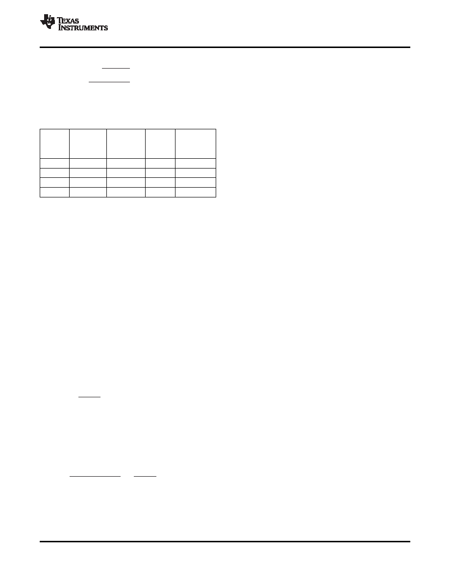
Table 2. Efficiency and Maximum Ambient
Temperature vs Output Power in 5-V 8- BTL
Systems
Equation 14 shows that the maximum ambient
Power
Max
Output
Internal
temperature is 53.3°C at maximum power dissipation
Efficiency
From
Ambient
Power
Dissipation
with a 5-V supply.
(%)
Supply Temperature
(W)
(°C)
Table 2 shows that for most applications no airflow is
0.25
31.4
0.55
0.75
62
required
to
keep
junction
temperatures
in
the
0.50
44.4
0.62
1.12
54
specified range. The TPA6205A1 is designed with
1.00
62.8
0.59
1.59
58
thermal protection that turns the device off when the
junction temperature surpasses 150°C to prevent
1.25
70.2
0.53
1.78
65
damage to the IC. Also, using more resistive than 8-
Table 2 employs Equation 11 to calculate efficiencies
speakers
dramatically
increases
the
thermal
for four different output power levels. Note that the
performance by reducing the output current.
efficiency of the amplifier is quite low for lower power
levels and rises sharply as power to the load is
increased resulting in a nearly flat internal power
For
the
DRB
(QFN/SON)
and
DGN
(MSOP)
dissipation over the normal operating range. Note that
packages, it is good practice to minimize the
the internal dissipation at full output power is less
presence of voids within the exposed thermal pad
than in the half power range. Calculating the
interconnection. Total elimination is difficult, but the
efficiency for a specific system is the key to proper
design of the exposed pad stencil is key. The stencil
power supply design. For a 1.25-W audio system with
design proposed in the Texas Instruments application
8-
loads and a 5-V supply, the maximum draw on
note
"QFN/SON
PCB
Attachment"
(SLUA271)
the power supply is almost 1.8 W.
enables out-gassing of the solder paste during reflow
A final point to remember about Class-AB amplifiers
as well as regulating the finished solder thickness.
is how to manipulate the terms in the efficiency
Typically the solder paste coverage is approximately
equation to the utmost advantage when possible.
50% of the pad area.
In making the pad size for the BGA balls, it is
This indicates that as VDD goes down, efficiency goes
recommended
that
the
layout
use
solder-
up.
mask-defined (SMD) land. With this method, the
A simple formula for calculating the maximum power
copper pad is made larger than the desired land area,
dissipated, PDmax, may be used for a differential
and the opening size is defined by the opening in the
output application:
solder mask material. The advantages normally
associated with this technique include more closely
controlled size and better copper adhesion to the
laminate.
Increased
copper
also
increases
the
thermal performance of the IC. Better size control is
PDmax for a 5-V, 8- system is 634 mW.
the result of photo imaging the stencils for masks.
Small plated vias should be placed near the center
The maximum ambient temperature depends on the
ball connecting ball B2 to the ground plane. Added
heat sinking ability of the PCB system. The derating
plated vias and ground plane act as a heatsink and
factor for the 2 mm x 2 mm Microstar Junior
increase the thermal performance of the device.
package is shown in the dissipation rating table.
Figure 35 shows the appropriate diameters for a 2
Converting this to
θ
JA:
mm × 2 mm MicroStar Junior BGA layout.
It is very important to keep the TPA6205A1 external
components very close to the TPA6205A1 to limit
Given
θ
JA,
the
maximum
allowable
junction
noise pickup. The TPA6205A1 evaluation module
(EVM) layout is shown in the next section as a layout
example.
Copyright 2006–2008, Texas Instruments Incorporated
15
Product Folder Link(s): TPA6205A1
相关PDF资料 |
PDF描述 |
|---|---|
| TPA6205A1DRBTG4 | 1.25 W, 1 CHANNEL, AUDIO AMPLIFIER, PDSO8 |
| TPA6205A1ZQVRG1 | 1.25 W, 1 CHANNEL, AUDIO AMPLIFIER, PBGA8 |
| TPA6205A1DRB | 1.25 W, 1 CHANNEL, AUDIO AMPLIFIER, PDSO8 |
| TPA6211A1DGNR | 2.45 W, 1 CHANNEL, AUDIO AMPLIFIER, PDSO8 |
| TPA6211A1DGN | 2.45 W, 1 CHANNEL, AUDIO AMPLIFIER, PDSO8 |
相关代理商/技术参数 |
参数描述 |
|---|---|
| TPA6205A1DRBT | 功能描述:音频放大器 1.25-W Mono Fully Diff Class-AB Aud RoHS:否 制造商:STMicroelectronics 产品:General Purpose Audio Amplifiers 输出类型:Digital 输出功率: THD + 噪声: 工作电源电压:3.3 V 电源电流: 最大功率耗散: 最大工作温度: 安装风格:SMD/SMT 封装 / 箱体:TQFP-64 封装:Reel |
| TPA6205A1DRBTG4 | 功能描述:音频放大器 1.25W Mono Fully Diff ClassAB Aud Amp RoHS:否 制造商:STMicroelectronics 产品:General Purpose Audio Amplifiers 输出类型:Digital 输出功率: THD + 噪声: 工作电源电压:3.3 V 电源电流: 最大功率耗散: 最大工作温度: 安装风格:SMD/SMT 封装 / 箱体:TQFP-64 封装:Reel |
| TPA6205A1EVM | 功能描述:音频 IC 开发工具 HEADPHONE DRIVER RoHS:否 制造商:Texas Instruments 产品:Evaluation Kits 类型:Audio Amplifiers 工具用于评估:TAS5614L 工作电源电压:12 V to 38 V |
| TPA6205A1ZQVR | 功能描述:音频放大器 1.25W Mono Fully Diff ClassAB Aud Amp RoHS:否 制造商:STMicroelectronics 产品:General Purpose Audio Amplifiers 输出类型:Digital 输出功率: THD + 噪声: 工作电源电压:3.3 V 电源电流: 最大功率耗散: 最大工作温度: 安装风格:SMD/SMT 封装 / 箱体:TQFP-64 封装:Reel |
| TPA6205A1ZQVRG1 | 功能描述:音频放大器 1.25W Mon,Fully Diff Class-AB Audio Amp RoHS:否 制造商:STMicroelectronics 产品:General Purpose Audio Amplifiers 输出类型:Digital 输出功率: THD + 噪声: 工作电源电压:3.3 V 电源电流: 最大功率耗散: 最大工作温度: 安装风格:SMD/SMT 封装 / 箱体:TQFP-64 封装:Reel |
发布紧急采购,3分钟左右您将得到回复。