- 您现在的位置:买卖IC网 > PDF目录98279 > TPS2300IPWRG4 (TEXAS INSTRUMENTS INC) 2-CHANNEL POWER SUPPLY SUPPORT CKT, PDSO20 PDF资料下载
参数资料
| 型号: | TPS2300IPWRG4 |
| 厂商: | TEXAS INSTRUMENTS INC |
| 元件分类: | 电源管理 |
| 英文描述: | 2-CHANNEL POWER SUPPLY SUPPORT CKT, PDSO20 |
| 封装: | GREEN, PLASTIC, TSSOP-20 |
| 文件页数: | 19/24页 |
| 文件大小: | 643K |
| 代理商: | TPS2300IPWRG4 |
www.ti.com
ABSOLUTE MAXIMUM RATINGS
DISSIPATION RATING TABLE
SLVS265G – FEBRUARY 2000 – REVISED NOVEMBER 2006
DETAILED DESCRIPTION (continued)
PWRGD1, PWRGD2 – PWRGD1 and PWRGD2 signal the presence of undervoltage conditions on VSENSE1
and VSENSE2, respectively. These pins are open-drain outputs and are pulled low during an undervoltage
condition. To minimize erroneous PWRGDx responses from transients on the voltage rail, the voltage sense
circuit incorporates a 20-
s deglitch filter. When VSENSEx is lower than the reference voltage (about 1.23 V),
PWRGDx is active low to indicate an undervoltage condition on the power-rail voltage. PWRGDx may not
correctly report power conditions when the device is disabled, because there is no gate drive power for the
PWRGD output transistor in the disable mode, or, in other words, PWRGD is floating. Therefore, PWRGD is
pulled up to its pullup power supply rail in disable mode.
TIMER – A capacitor on TIMER sets the time during which the power switch can be in overcurrent before turning
off. When the overcurrent protection circuits sense an excessive current, a current source is enabled which
charges the capacitor on TIMER. Once the voltage on TIMER reaches approximately 0.5 V, the circuit-breaker
latch is set and the power switch is latched off. Power must be recycled or the ENABLE pin must be toggled to
restart the controller. In high-power or high-temperature applications, a minimum 50-pF capacitor is strongly
recommended from TIMER to ground, to prevent any false triggering.
VREG – VREG is the output of an internal low-dropout voltage regulator, where IN1 is the input. The regulator is
used to generate a regulated voltage source, less than 5.5 V, for the device. A 0.1-
F ceramic capacitor should
be connected between VREG and ground to aid in noise rejection. In this configuration, upon disabling the
device, the internal low-dropout regulator will also be disabled, which removes power from the internal circuitry
and allows the device to be placed in low-quiescent-current mode. In applications where IN1 is less than 5.5 V,
VREG and IN1 may be connected together. However, under these conditions, disabling the device does not
place the device in low-quiescent-current mode, because the internal low-dropout voltage regulator is being
bypassed, thereby keeping internal circuitry operational. If VREG and IN1 are connected together, a 0.1-
F
ceramic capacitor between VREG and ground is not needed if IN1 already has a bypass capacitor of 1
F to
10
F.
VSENSE1, VSENSE2 – VSENSE1 and VSENSE2 can be used to detect undervoltage conditions on external
circuitry. If VSENSE1 senses a voltage below approximately 1.23 V, PWRGD1 is pulled low. Similarly, a voltage
less than 1.23 V on VSENSE2 causes PWRGD2 to be pulled low.
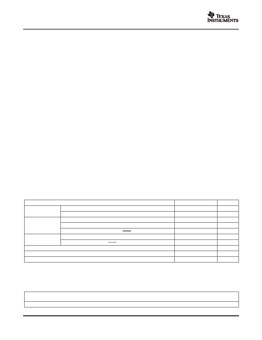
over operating free-air temperature range (unless otherwise noted) (1)(2)
VALUE
UNIT
VI(IN1), VI(ISENSE1), VI(VSENSE1), VI(VSENSE2), VI(ISET1), VI(ENABLE), VI(VREG)
–0.3 to 15
V
Input voltage range
VI(IN2), VI(ISENSE2), VI(ISET2)
–0.3 to 7
V
VO(GATE1)
–0.3 to 30
V
Output voltage range
VO(GATE2)
–0.3 to 22
V
VO(DISCH1), VO(PWRGD1), VO(PWRGD2), VO(FAULT), VO(DISCH2), VO(TIMER)
–0.3 to 15
V
I(GATE1), I(GATE2), I(DISCH1), I(DISCH2)
0 to 100
mA
Sink current range
I(PWRGD1), I(PWRGD2), I(TIMER), I(FAULT)
0 to 10
mA
Operating virtual junction temperature range, TJ
–40 to 100
°C
Storage temperature range, Tstg
–55 to 150
°C
Lead temperature 1,6 mm (1/16 inch) from case for 10 seconds
260
°C
(1)
Stresses beyond those listed under absolute maximum ratings may cause permanent damage to the device. These are stress ratings
only, and functional operation of the device at these or any other conditions beyond those indicated under recommended operating
conditions is not implied. Exposure to absolute-maximum-rated conditions for extended periods may affect device reliability.
(2)
All voltages are respect to DGND.
TA ≤ 25°C
DERATING FACTOR
TA = 70°C
TA = 85°C
PACKAGE
POWER RATING
ABOVE TA = 25°C
POWER RATING
PW-20
1015 mW
13.55 mW/
°C
406 mW
203 mW
4
相关PDF资料 |
PDF描述 |
|---|---|
| TPS2306DWG4 | 2-CHANNEL POWER SUPPLY SUPPORT CKT, PDSO16 |
| TPS2340APFPRG4 | 2-CHANNEL POWER SUPPLY SUPPORT CKT, PQFP80 |
| TPS2341PHPR | 4-CHANNEL POWER SUPPLY SUPPORT CKT, PQFP48 |
| TPS2343DDPG3 | 6-CHANNEL POWER SUPPLY SUPPORT CKT, PDSO80 |
| TPS2343DDPR | 6-CHANNEL POWER SUPPLY SUPPORT CKT, PDSO80 |
相关代理商/技术参数 |
参数描述 |
|---|---|
| TPS2301EVM-153 | 功能描述:电源管理IC开发工具 TPS23XX Hot Swap Pow Contrs Eval Mod RoHS:否 制造商:Maxim Integrated 产品:Evaluation Kits 类型:Battery Management 工具用于评估:MAX17710GB 输入电压: 输出电压:1.8 V |
| TPS2301IPW | 功能描述:热插拔功率分布 3-13V Dual w/Ind Chl Circuit Breaking RoHS:否 制造商:Texas Instruments 产品:Controllers & Switches 电流限制: 电源电压-最大:7 V 电源电压-最小:- 0.3 V 工作温度范围: 功率耗散: 安装风格:SMD/SMT 封装 / 箱体:MSOP-8 封装:Tube |
| TPS2301IPWG4 | 功能描述:热插拔功率分布 3-13V Dual w/Ind Chl Circuit Breaking RoHS:否 制造商:Texas Instruments 产品:Controllers & Switches 电流限制: 电源电压-最大:7 V 电源电压-最小:- 0.3 V 工作温度范围: 功率耗散: 安装风格:SMD/SMT 封装 / 箱体:MSOP-8 封装:Tube |
| TPS2301IPWR | 功能描述:热插拔功率分布 3-13V Dual w/Ind Chl Circuit Breaking RoHS:否 制造商:Texas Instruments 产品:Controllers & Switches 电流限制: 电源电压-最大:7 V 电源电压-最小:- 0.3 V 工作温度范围: 功率耗散: 安装风格:SMD/SMT 封装 / 箱体:MSOP-8 封装:Tube |
| TPS2301IPWRG4 | 功能描述:热插拔功率分布 3-13V Dual w/Ind Chl Circuit Breaking RoHS:否 制造商:Texas Instruments 产品:Controllers & Switches 电流限制: 电源电压-最大:7 V 电源电压-最小:- 0.3 V 工作温度范围: 功率耗散: 安装风格:SMD/SMT 封装 / 箱体:MSOP-8 封装:Tube |
发布紧急采购,3分钟左右您将得到回复。