- 您现在的位置:买卖IC网 > PDF目录69504 > TPS2410PW (TEXAS INSTRUMENTS INC) SPECIALTY ANALOG CIRCUIT, PDSO14 PDF资料下载
参数资料
| 型号: | TPS2410PW |
| 厂商: | TEXAS INSTRUMENTS INC |
| 元件分类: | 模拟信号调理 |
| 英文描述: | SPECIALTY ANALOG CIRCUIT, PDSO14 |
| 封装: | GREEN, PLASTIC, TSSOP-14 |
| 文件页数: | 4/31页 |
| 文件大小: | 1020K |
| 代理商: | TPS2410PW |
第1页第2页第3页当前第4页第5页第6页第7页第8页第9页第10页第11页第12页第13页第14页第15页第16页第17页第18页第19页第20页第21页第22页第23页第24页第25页第26页第27页第28页第29页第30页第31页
APPLICATION INFORMATION
OVERVIEW
Gate
ON
Gate
OFF
1
0
m
V
3
m
V
Programmable
FastTurn-off
Threshold
Gnd
1
0
m
V
3
m
V
Programmable
FastTurn-off
Threshold
Active
Regulation
SlowTurn-off
Range
TPS2411
(SeeText)
TPS2410
(SeeText)
V
+10V
(A)
V
+V
(A)
(T)
V(AC)
V
(G
A
TE)
V
(G
A
TE)
SLVS727C – NOVEMBER 2006 – REVISED JUNE 2009 .................................................................................................................................................. www.ti.com
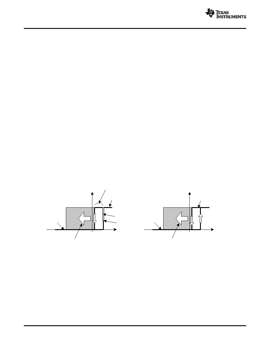
The TPS2410/11 is designed to allow output ORing in N+1 power supply applications (see Figure 12) and
input-power bus ORing in redundant source applications (see Figure 13). The TPS2410/11 and external
MOSFET emulate a discrete diode to perform this unidirectional power combining function. The advantage to this
emulation is lower forward voltage drop and the ability to tune operation.
The TPS2410 turns the MOSFET on with a linear control loop that regulates V(AC) to 10 mV as shown in
Figure 11. With the gate low, and V(AC) increasing to 10 mV, the amplifier drives GATE high with all available
output current until regulation is reached. The regulator controls V(GATE) to maintain V(AC) at 10 mV as long as the
MOSFET rDS(on) × I(DRAIN) is less than this the regulated voltage. The regulator drives GATE high, turning the
MOSFET fully ON when the rDS(on) × I(DRAIN) exceeds 10 mV, otherwise V(GATE) will be near V(A) plus the
MOSFET gate threshold voltage. If the external circuits force V(AC) below 10 mV and above the programmed fast
turnoff, GATE is slowly turned off. GATE is rapidly pulled to ground if V(AC) falls to the RSET programmed fast
turn-off threshold.
The TPS2411 turns the MOSFET on and off like a comparator with hysteresis as shown in Figure 11. GATE is
driven high when V(AC) exceeds 10 mV, and rapidly turned off if V(AC) falls to the RSET programmed fast turn-off
threshold.
System designs should account for the inherent delay between a TPS2410/11 circuit becoming forward biased,
and the MOSFET actually turning ON. The delay is the result of the MOSFET gate capacitance charge from
ground to its threshold voltage by the 270
A gate current. If there are no additional sources holding the ORed
rail voltage up, the MOSFET internal diode will conduct and maintain voltage on the ORed output, but there will
be some voltage droop. This condition is analogous to the power source being ORed in this case. The DC/DC
converter output voltage droops when its load increases from zero to a high value. Load sharing techniques that
keep all ORed sources active solve this condition.
Figure 11. TPS2410/11 Operation
12
Copyright 2006–2009, Texas Instruments Incorporated
Product Folder Link(s): TPS2410 TPS2411
相关PDF资料 |
PDF描述 |
|---|---|
| TPS2411PWG4 | SPECIALTY ANALOG CIRCUIT, PDSO14 |
| TPS2412PWR | SPECIALTY ANALOG CIRCUIT, PDSO8 |
| TPS2412DG4 | SPECIALTY ANALOG CIRCUIT, PDSO8 |
| TPS2413D | SPECIALTY ANALOG CIRCUIT, PDSO8 |
| TPS2413PWR | SPECIALTY ANALOG CIRCUIT, PDSO8 |
相关代理商/技术参数 |
参数描述 |
|---|---|
| TPS2410PW | 制造商:Texas Instruments 功能描述:Hot Swap Controller IC |
| TPS2410PWG4 | 功能描述:热插拔功率分布 N+1 and OR-ing Pwr Rail Controller RoHS:否 制造商:Texas Instruments 产品:Controllers & Switches 电流限制: 电源电压-最大:7 V 电源电压-最小:- 0.3 V 工作温度范围: 功率耗散: 安装风格:SMD/SMT 封装 / 箱体:MSOP-8 封装:Tube |
| TPS2410PWR | 功能描述:热插拔功率分布 N+1 OR-ing Pwr Rail Cntrlr RoHS:否 制造商:Texas Instruments 产品:Controllers & Switches 电流限制: 电源电压-最大:7 V 电源电压-最小:- 0.3 V 工作温度范围: 功率耗散: 安装风格:SMD/SMT 封装 / 箱体:MSOP-8 封装:Tube |
| TPS2410PWR/2801 | 功能描述:热插拔功率分布 Oring Controller RoHS:否 制造商:Texas Instruments 产品:Controllers & Switches 电流限制: 电源电压-最大:7 V 电源电压-最小:- 0.3 V 工作温度范围: 功率耗散: 安装风格:SMD/SMT 封装 / 箱体:MSOP-8 封装:Tube |
| TPS2410PWRG4 | 功能描述:热插拔功率分布 N+1 and OR-ing Pwr Rail Controller RoHS:否 制造商:Texas Instruments 产品:Controllers & Switches 电流限制: 电源电压-最大:7 V 电源电压-最小:- 0.3 V 工作温度范围: 功率耗散: 安装风格:SMD/SMT 封装 / 箱体:MSOP-8 封装:Tube |
发布紧急采购,3分钟左右您将得到回复。