- 您现在的位置:买卖IC网 > PDF目录199467 > TPS40222DRPTG4 (TEXAS INSTRUMENTS INC) 3.5 A SWITCHING REGULATOR, 1500 kHz SWITCHING FREQ-MAX, PDSO6 PDF资料下载
参数资料
| 型号: | TPS40222DRPTG4 |
| 厂商: | TEXAS INSTRUMENTS INC |
| 元件分类: | 稳压器 |
| 英文描述: | 3.5 A SWITCHING REGULATOR, 1500 kHz SWITCHING FREQ-MAX, PDSO6 |
| 封装: | 3 X 3 MM, GREEN, PLASTIC, VSON-6 |
| 文件页数: | 6/27页 |
| 文件大小: | 662K |
| 代理商: | TPS40222DRPTG4 |
第1页第2页第3页第4页第5页当前第6页第7页第8页第9页第10页第11页第12页第13页第14页第15页第16页第17页第18页第19页第20页第21页第22页第23页第24页第25页第26页第27页
www.ti.com
4
3
6
5
1
0
2
20
0
60
70
80
10
30
40
50
COUT Output Capacitance F
L = 5.6
H
V
O
U
T
Output
V
oltage
V
PHASE = 50
°
L = 2.2
H
0
20
40
60
80
100
120
0
20
100
40
70
10
90
30
60
50
Phase
Margin
°
COUT Output Capacitance F
L = 1.8
H
VOUT = 1.8 V
L = 5.6
H
C
LEAD +
1
2 p
f
R
(8)
f
R +
1
2 p
1
L
C
O
1
2
(9)
Catch Diode (D1)
SLUS642A – OCTOBER 2005 – REVISED JANUARY 2006
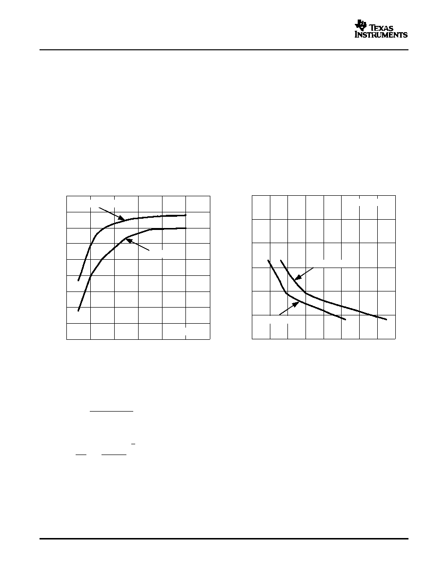
These component selection decisions influence the phase margin and hence the stability of the system. For
example, raising the output capacitance reduces the system crossover frequency and raises phase margin.
Figure 11 illustrates this in a curve that shows phase margin as a function of output capacitance for two widely
different inductors. The curves show that beyond a certain point, added capacitance has limited benefit. This
point can be exploited to avoid the expense of excessive output capacitance. The curves also show the
advantage of a lower inductance, where only 20-
F of output capacitance is required to obtain 60 degrees of
phase margin.
The output voltage affects the phase margin by changing the equivalent output resistance to deliver full load.
With a higher output voltage for example, there is a higher full-load resistance and a lower output capacitance is
required for the same phase margin. An idea of this effect is illustrated in Figure 12 which plots the required
minimum capacitance to achieve 50 degrees of phase margin at different output voltages. The curves also show
the reduction in output capacitance that may be achieved with a lower inductor value.
PHASE MARGIN
OUTPUT VOLTAGE
vs
OUTPUT CAPACITANCE
Figure 11.
Figure 12.
A further improvement in reducing output capacitance is made by adding a lead capacitor across R1 of the
feedback network. This lead capacitor can be determined by making its impedance equal to the resistance of R1
at the resonant frequency of the output L-C network. The lead capacitance is calculated using Equation 8.
The resonant frequency formed by the inductor and the output load capacitance is calculated in Equation 9.
The selection of the catch diode depends on the application current. Select a diode that has a low forward
voltage drop, and a low junction capacitance. A diode with too high of a forward voltage drop or a diode with high
junction capacitance result in a converter that has poor efficiency, as well as excessive ringing on the SW node
and excessive output voltage noise.
14
相关PDF资料 |
PDF描述 |
|---|---|
| TPS5103IDBG4 | 3 A SWITCHING CONTROLLER, 500 kHz SWITCHING FREQ-MAX, PDSO20 |
| TPS54680PWP | 12 A SWITCHING REGULATOR, 762 kHz SWITCHING FREQ-MAX, PDSO28 |
| TPS54872PWP | 12 A SWITCHING REGULATOR, 762 kHz SWITCHING FREQ-MAX, PDSO28 |
| TPS54972PWP | 16 A SWITCHING REGULATOR, 762 kHz SWITCHING FREQ-MAX, PDSO28 |
| TPS5510D | 1-CHANNEL POWER SUPPLY SUPPORT CKT, PDSO8 |
相关代理商/技术参数 |
参数描述 |
|---|---|
| TPS40222EVM-001 | 功能描述:电源管理IC开发工具 Non-Sync Buck Conv Eval Mod RoHS:否 制造商:Maxim Integrated 产品:Evaluation Kits 类型:Battery Management 工具用于评估:MAX17710GB 输入电压: 输出电压:1.8 V |
| TPS40-23 | 制造商:TOTAL-POWER 制造商全称:TOTAL-POWER 功能描述:40 WATT OPEN - FRAME SWITCHING POWER SUPPLY |
| TPS40-24 | 制造商:TOTAL-POWER 制造商全称:TOTAL-POWER 功能描述:40 WATT OPEN - FRAME SWITCHING POWER SUPPLY |
| TPS40-25 | 制造商:TOTAL-POWER 制造商全称:TOTAL-POWER 功能描述:40 WATT OPEN - FRAME SWITCHING POWER SUPPLY |
| TPS40-30 | 制造商:TOTAL-POWER 制造商全称:TOTAL-POWER 功能描述:40 WATT OPEN - FRAME SWITCHING POWER SUPPLY |
发布紧急采购,3分钟左右您将得到回复。