- 您现在的位置:买卖IC网 > PDF目录98282 > TPS54073PWPR (TEXAS INSTRUMENTS INC) 25 A SWITCHING REGULATOR, 762 kHz SWITCHING FREQ-MAX, PDSO28 PDF资料下载
参数资料
| 型号: | TPS54073PWPR |
| 厂商: | TEXAS INSTRUMENTS INC |
| 元件分类: | 稳压器 |
| 英文描述: | 25 A SWITCHING REGULATOR, 762 kHz SWITCHING FREQ-MAX, PDSO28 |
| 封装: | GREEN, PLASTIC, HTSSOP-28 |
| 文件页数: | 25/26页 |
| 文件大小: | 850K |
| 代理商: | TPS54073PWPR |
APPLICATION INFORMATION
PCB LAYOUT
AGND
BOOT
VSENSE
COMP
PWRGD
PH
RT
SYNC
SS/ENA
VBIAS
VIN
PVIN
PGND
VOUT
PH
PVIN
TOPSIDEGROUND AREA
VIA toGroundPlane
ANALOGGROUND TRACE
EXPOSED
POWERPAD
AREA
COMPENSATION
NETWORK
OUTPUT INDUCTOR
OUTPUT
FILTER
CAPACITOR
BOOT
CAPACITOR
INPUT
BYPASS
CAPACITOR
INPUT
BULK
FILTER
FREQUENCY SET RESISTOR
SLOWSTART
CAPACITOR
BIASCAPACITOR
INPUT
BYPASS
CAPACITOR
VIN
OPTIONAL PRE-CHARGEDIODES
CONNECT TOPRE-CHARGE
VOLTAGESOURCE
SLVS547 – FEBRUARY 2005 ............................................................................................................................................................................................ www.ti.com
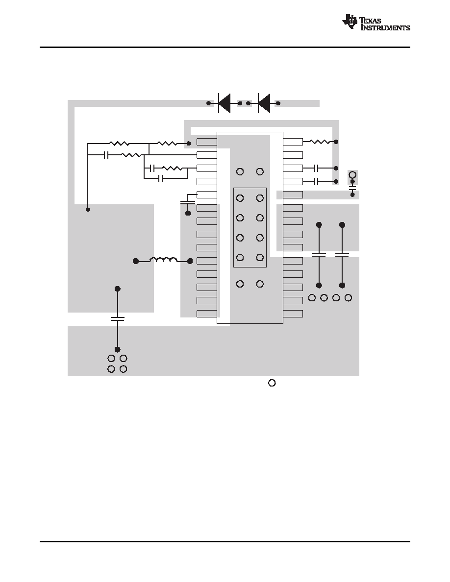
Figure 10. TPS54073 Layout
The PVIN pins are connected together on the printed-
additional vias at the ground side of the input and
circuit board (PCB) and bypassed with a low ESR
output filter capacitors. The AGND and PGND pins
ceramic bypass capacitor. Care should be taken to
are tied to the PCB ground by connecting them to the
minimize the loop area formed by the bypass
ground area under the device as shown in Figure 10.
capacitor connections, the PVIN pins, and the
Use a separate wide trace for the analog ground
TPS54073 ground pins. The minimum recommended
signal path. This analog ground is used for the
bypass capacitance is a 10-
F ceramic capacitor with
voltage set point divider, timing resistor RT, slow-start
a X5R or X7R dielectric. The optimum placement is
capacitor, and bias capacitor grounds. The PH pins
as close as possible to the PVIN pins, the AGND,
are tied together and routed to the output inductor.
and PGND pins. See Figure 10 for an example of a
Because the PH connection is the switching node, an
board layout. If the VIN is connected to a separate
inductor is located close to the PH pins, and the area
source supply, it is bypassed with its own capacitor.
of the PCB conductor is minimized to prevent
There is an area of ground on the top layer of the
excessive capacitive coupling. Connect the boot
PCB, directly under the IC, with an exposed area for
capacitor between the phase node and the BOOT pin
connection to the PowerPAD. Use vias to connect
as shown in Figure 10. Keep the boot capacitor close
this ground area to any internal ground planes. Use
to the IC, and minimize the conductor trace lengths.
8
Copyright 2005, Texas Instruments Incorporated
Product Folder Link(s): TPS54073
相关PDF资料 |
PDF描述 |
|---|---|
| TPS54073PWP | 25 A SWITCHING REGULATOR, 762 kHz SWITCHING FREQ-MAX, PDSO28 |
| TPS5410QDRQ1 | SWITCHING REGULATOR, PDSO8 |
| TPS54110PWP | 3.5 A SWITCHING REGULATOR, 762 kHz SWITCHING FREQ-MAX, PDSO20 |
| TPS54110PWPG4 | 3.5 A SWITCHING REGULATOR, 762 kHz SWITCHING FREQ-MAX, PDSO20 |
| TPS54140QDRCRQ1 | SWITCHING REGULATOR, PDSO10 |
相关代理商/技术参数 |
参数描述 |
|---|---|
| TPS54073PWPRG4 | 功能描述:直流/直流开关调节器 2.2V-4.0V 14A Sync Buck Converter RoHS:否 制造商:International Rectifier 最大输入电压:21 V 开关频率:1.5 MHz 输出电压:0.5 V to 0.86 V 输出电流:4 A 输出端数量: 最大工作温度: 安装风格:SMD/SMT 封装 / 箱体:PQFN 4 x 5 |
| TPS5410 | 制造商:TI 制造商全称:Texas Instruments 功能描述:1-A, WIDE INPUT RANGE, STEP-DOWN SWIFT CONVERTER |
| TPS5410D | 功能描述:直流/直流开关调节器 5.5V to 36V Input 1A Step Down Conv RoHS:否 制造商:International Rectifier 最大输入电压:21 V 开关频率:1.5 MHz 输出电压:0.5 V to 0.86 V 输出电流:4 A 输出端数量: 最大工作温度: 安装风格:SMD/SMT 封装 / 箱体:PQFN 4 x 5 |
| TPS5410DG4 | 功能描述:直流/直流开关调节器 5.5V to 36V Input 1A Step Down Conv RoHS:否 制造商:International Rectifier 最大输入电压:21 V 开关频率:1.5 MHz 输出电压:0.5 V to 0.86 V 输出电流:4 A 输出端数量: 最大工作温度: 安装风格:SMD/SMT 封装 / 箱体:PQFN 4 x 5 |
| TPS5410DR | 功能描述:直流/直流开关调节器 5.5V-36V Input 1A Step Down Converter RoHS:否 制造商:International Rectifier 最大输入电压:21 V 开关频率:1.5 MHz 输出电压:0.5 V to 0.86 V 输出电流:4 A 输出端数量: 最大工作温度: 安装风格:SMD/SMT 封装 / 箱体:PQFN 4 x 5 |
发布紧急采购,3分钟左右您将得到回复。