- 您现在的位置:买卖IC网 > PDF目录69511 > TPS54331QDRQ1 (TEXAS INSTRUMENTS INC) 2 A SWITCHING REGULATOR, 684 kHz SWITCHING FREQ-MAX, PDSO8 PDF资料下载
参数资料
| 型号: | TPS54331QDRQ1 |
| 厂商: | TEXAS INSTRUMENTS INC |
| 元件分类: | 稳压器 |
| 英文描述: | 2 A SWITCHING REGULATOR, 684 kHz SWITCHING FREQ-MAX, PDSO8 |
| 封装: | GREEN, PLASTIC, DSO-8 |
| 文件页数: | 10/25页 |
| 文件大小: | 735K |
| 代理商: | TPS54331QDRQ1 |
BOOT
VSENSE
PH
VIN
GND
EN
Vout
PH
Vin
TOPSIDE
GROUND
AREA
OUTPUT
INDUCTOR
OUTPUT
FILTER
CAPACITOR
BOOT
CAPACITOR
INPUT
BYPASS
CAPACITOR
CATCH
DIODE
SignalVIA
RouteBOOT CAPACITOR
traceonotherlayertoprovide
widepathfortopsideground
RESISTOR
DIVIDER
Feedback Trace
COMP
SS
COMPENSATION
NETWORK
ThermalVIA
SLOWSTART
CAPACITOR
UVLO
RESISTOR
DIVIDER
SLVSAB5 – NOVEMBER 2010
www.ti.com
Ptot is the total device power dissipation (W).
TA is the ambient temperature (°C).
TJ is the junction temperature (°C) .
Rth is the thermal resistance of the package (°C/W).
TJMAX is maximum junction temperature (°C).
TAMAX is maximum ambient temperature (°C).
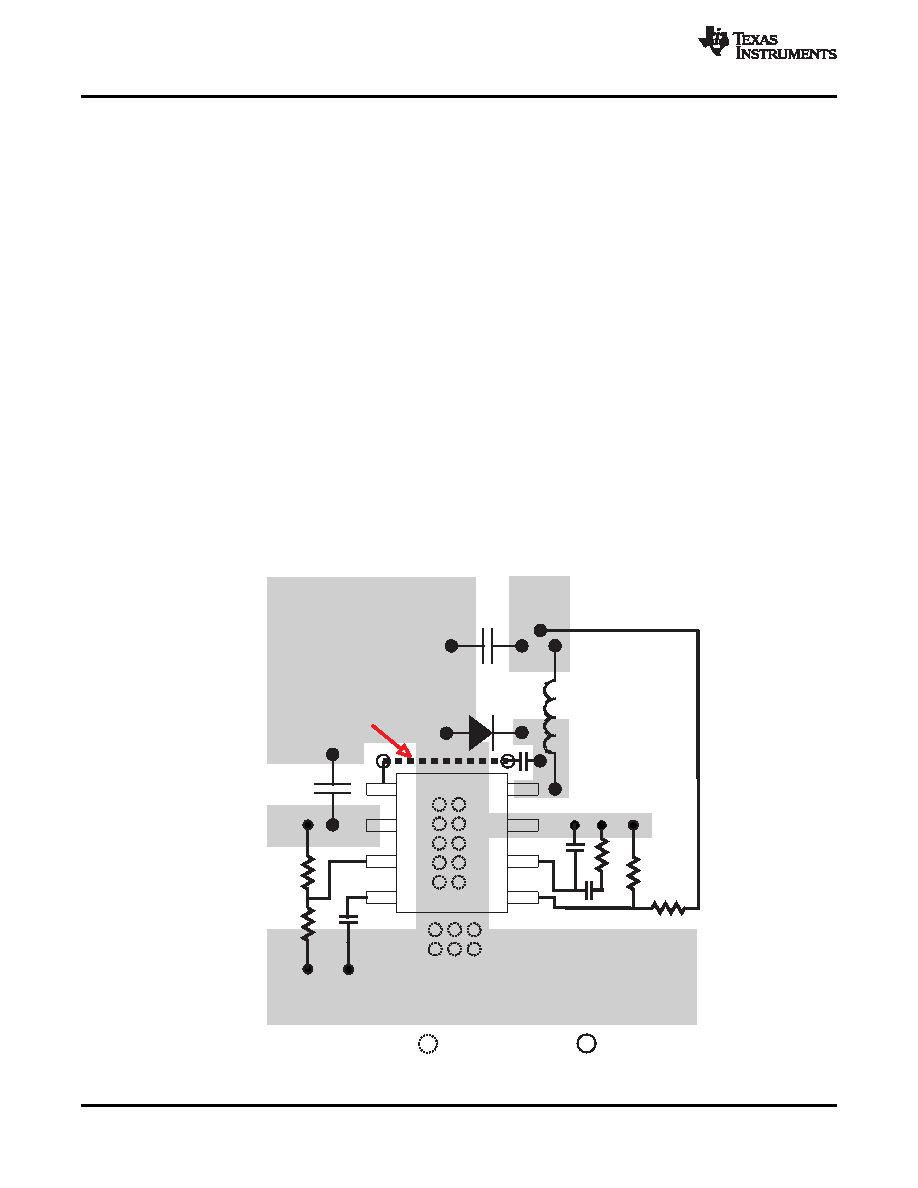
PCB LAYOUT
The VIN pin should be bypassed to ground with a low ESR ceramic bypass capacitor. Care should be taken to
minimize the loop area formed by the bypass capacitor connections, the VIN pin, and the anode of the catch
diode. The typical recommended bypass capacitance is 10-mF ceramic with a X5R or X7R dielectric and the
optimum placement is closest to the VIN pins and the source of the anode of the catch diode. See Figure 14 for
a PCB layout example. The GND D pin should be tied to the PCB ground plane at the pin of the IC. The source
of the low-side MOSFET should be connected directly to the top side PCB ground area used to tie together the
ground sides of the input and output capacitors as well as the anode of the catch diode. The PH pin should be
routed to the cathode of the catch diode and to the output inductor. Since the PH connection is the switching
node, the catch diode and output inductor should be located very close to the PH pins, and the area of the PCB
conductor minimized to prevent excessive capacitive coupling. For operation at full rated load, the top side
ground area must provide adequate heat dissipating area. The TPS54331 uses a fused lead frame so that the
GND pin acts as a conductive path for heat dissipation from the die. Many applications have larger areas of
internal or back side ground plane available, and the top side ground area can be connected to these areas
using multiple vias under or adjacent to the device to help dissipate heat. The additional external components
can be placed approximately as shown. It may be possible to obtain acceptable performance with alternate
layout schemes, however this layout has been shown to produce good results and is intended as a guideline.
Figure 14. TPS54331 Board Layout
18
Copyright 2010, Texas Instruments Incorporated
Product Folder Link(s): TPS54331-Q1
相关PDF资料 |
PDF描述 |
|---|---|
| TPS54332DDAR | SWITCHING REGULATOR, 1200 kHz SWITCHING FREQ-MAX, PDSO8 |
| TPS54350PWPR | 6.5 A SWITCHING REGULATOR, 700 kHz SWITCHING FREQ-MAX, PDSO16 |
| TPS54350PWP | 6.5 A SWITCHING REGULATOR, 700 kHz SWITCHING FREQ-MAX, PDSO16 |
| TPS54355PWPRG4 | 6.5 A SWITCHING REGULATOR, 600 kHz SWITCHING FREQ-MAX, PDSO16 |
| TPS54353PWPR | 6.5 A SWITCHING REGULATOR, 600 kHz SWITCHING FREQ-MAX, PDSO16 |
相关代理商/技术参数 |
参数描述 |
|---|---|
| TPS54332 | 制造商:TI 制造商全称:Texas Instruments 功能描述:3.5A, 28V, 1MHz, STEP DOWN DC/DC CONVERTER WITH Eco-modea?¢ |
| TPS54332DDA | 功能描述:直流/直流开关调节器 DC/DC Converter with Eco-mode RoHS:否 制造商:International Rectifier 最大输入电压:21 V 开关频率:1.5 MHz 输出电压:0.5 V to 0.86 V 输出电流:4 A 输出端数量: 最大工作温度: 安装风格:SMD/SMT 封装 / 箱体:PQFN 4 x 5 |
| TPS54332DDAR | 功能描述:直流/直流开关转换器 DC/DC Converter with Eco-mode RoHS:否 制造商:STMicroelectronics 最大输入电压:4.5 V 开关频率:1.5 MHz 输出电压:4.6 V 输出电流:250 mA 输出端数量:2 最大工作温度:+ 85 C 安装风格:SMD/SMT |
| TPS54332EVM-416 | 功能描述:电源管理IC开发工具 5-15V,3A,SWIFT Buck Converter Eval Mod RoHS:否 制造商:Maxim Integrated 产品:Evaluation Kits 类型:Battery Management 工具用于评估:MAX17710GB 输入电压: 输出电压:1.8 V |
| TPS54334DDA | 功能描述:Buck Switching Regulator IC Positive Adjustable 0.8V 1 Output 3A 8-PowerSOIC (0.154", 3.90mm Width) 制造商:texas instruments 系列:- 包装:管件 零件状态:有效 功能:降压 输出配置:正 拓扑:降压 输出类型:可调式 输出数:1 电压 - 输入(最小值):4.2V 电压 - 输入(最大值):28V 电压 - 输出(最小值/固定):0.8V 电压 - 输出(最大值):24V 电流 - 输出:3A 频率 - 开关:570kHz 同步整流器:是 工作温度:-40°C ~ 150°C(TJ) 安装类型:表面贴装 封装/外壳:8-PowerSOIC(0.154",3.90mm 宽) 供应商器件封装:8-SO PowerPad 标准包装:75 |
发布紧急采购,3分钟左右您将得到回复。