- 您现在的位置:买卖IC网 > PDF目录69512 > TPS54616QPWPRQ1 (TEXAS INSTRUMENTS INC) 12 A SWITCHING REGULATOR, 762 kHz SWITCHING FREQ-MAX, PDSO28 PDF资料下载
参数资料
| 型号: | TPS54616QPWPRQ1 |
| 厂商: | TEXAS INSTRUMENTS INC |
| 元件分类: | 稳压器 |
| 英文描述: | 12 A SWITCHING REGULATOR, 762 kHz SWITCHING FREQ-MAX, PDSO28 |
| 封装: | GREEN, PLASTIC, HTSSOP-28 |
| 文件页数: | 3/20页 |
| 文件大小: | 403K |
| 代理商: | TPS54616QPWPRQ1 |
TPS54611Q1,TPS54612Q1
TPS54613Q1,TPS54614Q1
TPS54615Q1,TPS54616Q1
SGLS266G OCTOBER 2004 REVISED JUNE 2008
www.ti.com
11
GROUNDING AND POWERPAD LAYOUT
The TPS5461116 have two internal grounds (analog and
power). Inside the TPS5461116, the analog ground ties
to all of the noise sensitive signals, while the power ground
ties to the noisier power signals. The PowerPAD is tied
internally to the analog ground. Noise injected between the
two grounds can degrade the performance of the
TPS5461116, particularly at higher output currents.
However, ground noise on an analog ground plane can
also cause problems with some of the control and bias
signals. For these reasons, separate analog and power
ground planes are recommended. These two planes
should tie together directly at the IC to reduce noise
between the two grounds. The only components that
should tie directly to the power ground plane are the input
capacitor, the output capacitor, the input voltage
decoupling capacitor, and the PGND pins of the
TPS5461116. The layout of the TPS54614 evaluation
module is representative of a recommended layout for a
4-layer
board.
Documentation
for
the
TPS54614
evaluation module can be found on the Texas Instruments
web site (www.ti.com) under the TPS54614 product folder.
See the TPS54614185 User’s Guide, Texas Instruments
(SLVU053) and the application note, Texas Instruments
(SLVA105).
LAYOUT CONSIDERATIONS FOR THERMAL
PERFORMANCE
For operation at full rated load current, the analog ground
plane must provide adequate heat dissipating area. A 3
inch by 3 inch plane of 1 ounce copper is recommended,
though not mandatory, depending on ambient temperature
and airflow. Most applications have larger areas of internal
ground plane available, and the PowerPAD should be
connected to the largest area available. Additional areas
on the top or bottom layers also help dissipate heat, and
any area available should be used when 3 A or greater
operation is desired. Connection from the exposes area of
the PowerPAD to the analog ground plane layer should be
made using 0.013 inch diameter vias to avoid solder
wicking through the vias. Six vias should be in the
PowerPAD area with four additional vias located under the
device package. The size of the vias under the package,
but not in the exposed thermal pad area, can be increased
to 0.018. Additional vias beyond the 10 recommended that
enhance thermal performance should be included in areas
not under the device package.
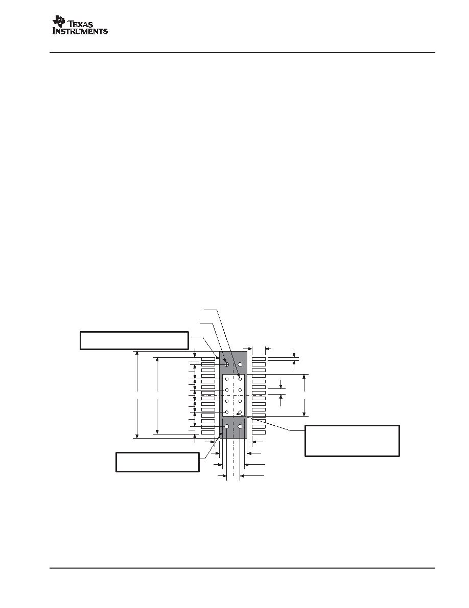
Connect Pin 1 to Analog Ground Plane
in This Area for Optimum Performance
Minimum Recommended Top
Side Analog Ground Area
0.3478
0.0150
0.06
0.0256
0.1700
0.1340
0.0630
0.0400
0.0180
4 PL
0.2090
0.0130
8 PL
Minimum Recommended Exposed
Copper Area for Powerpad. 5mm
Stencils May Require 10 Percent
Larger Area
0.0650
0.0500
0.0650
0.0339
0.0500
Minimum Recommended Thermal Vias: 8 x 0.013 Diameter Inside
Powerpad Area 4 x 0.018 Diameter Under Device as Shown.
Additional 0.018 Diameter Vias May Be Used if Top Side Analog Ground
Area Is Extended.
0.3820
Figure 11. Recommended Land Pattern for 28-Pin PWP PowerPAD
相关PDF资料 |
PDF描述 |
|---|---|
| TPS54613QPWPRQ1 | 12 A SWITCHING REGULATOR, 762 kHz SWITCHING FREQ-MAX, PDSO28 |
| TPS54614QPWPRQ1 | 12 A SWITCHING REGULATOR, 762 kHz SWITCHING FREQ-MAX, PDSO28 |
| TPS54617RUVT | SWITCHING REGULATOR, 660 kHz SWITCHING FREQ-MAX, QCC34 |
| TPS54620RHLT | SWITCHING REGULATOR, 1760 kHz SWITCHING FREQ-MAX, PQCC14 |
| TPS54620RHLR | SWITCHING REGULATOR, 1760 kHz SWITCHING FREQ-MAX, PQCC14 |
相关代理商/技术参数 |
参数描述 |
|---|---|
| TPS54617 | 制造商:TI 制造商全称:Texas Instruments 功能描述:3-V TO 6-V INPUT, 6-A, SMALL SYNCHRONOUS-BUCK SWITCHER WITH INTEGRATED FETs (SWIFT?) |
| TPS54617EVM-414 | 功能描述:电源管理IC开发工具 6A,3-6V Inp,SWIFT Converter Eval Mod RoHS:否 制造商:Maxim Integrated 产品:Evaluation Kits 类型:Battery Management 工具用于评估:MAX17710GB 输入电压: 输出电压:1.8 V |
| TPS54617EVM-414 | 制造商:Texas Instruments 功能描述:EVAL BOARD, TPS54617 1.8V, 6A SYNC STEP- |
| TPS54617RUV | 制造商:TI 制造商全称:Texas Instruments 功能描述:3-V TO 6-V INPUT, 6-A, SMALL SYNCHRONOUS-BUCK SWITCHER WITH INTEGRATED FETs (SWIFT?) |
| TPS54617RUVR | 功能描述:直流/直流开关调节器 3-6V 6A SWIFT Step Down DCDC Converter RoHS:否 制造商:International Rectifier 最大输入电压:21 V 开关频率:1.5 MHz 输出电压:0.5 V to 0.86 V 输出电流:4 A 输出端数量: 最大工作温度: 安装风格:SMD/SMT 封装 / 箱体:PQFN 4 x 5 |
发布紧急采购,3分钟左右您将得到回复。