- 您现在的位置:买卖IC网 > PDF目录69512 > TPS54617RUVT (TEXAS INSTRUMENTS INC) SWITCHING REGULATOR, 660 kHz SWITCHING FREQ-MAX, QCC34 PDF资料下载
参数资料
| 型号: | TPS54617RUVT |
| 厂商: | TEXAS INSTRUMENTS INC |
| 元件分类: | 稳压器 |
| 英文描述: | SWITCHING REGULATOR, 660 kHz SWITCHING FREQ-MAX, QCC34 |
| 封装: | 3.50 X 7 MM, GREEN, VQFN-34 |
| 文件页数: | 1/21页 |
| 文件大小: | 852K |
| 代理商: | TPS54617RUVT |
3,5mmx7mm
TypicalSize
1
FEATURES
DESCRIPTION
APPLICATIONS
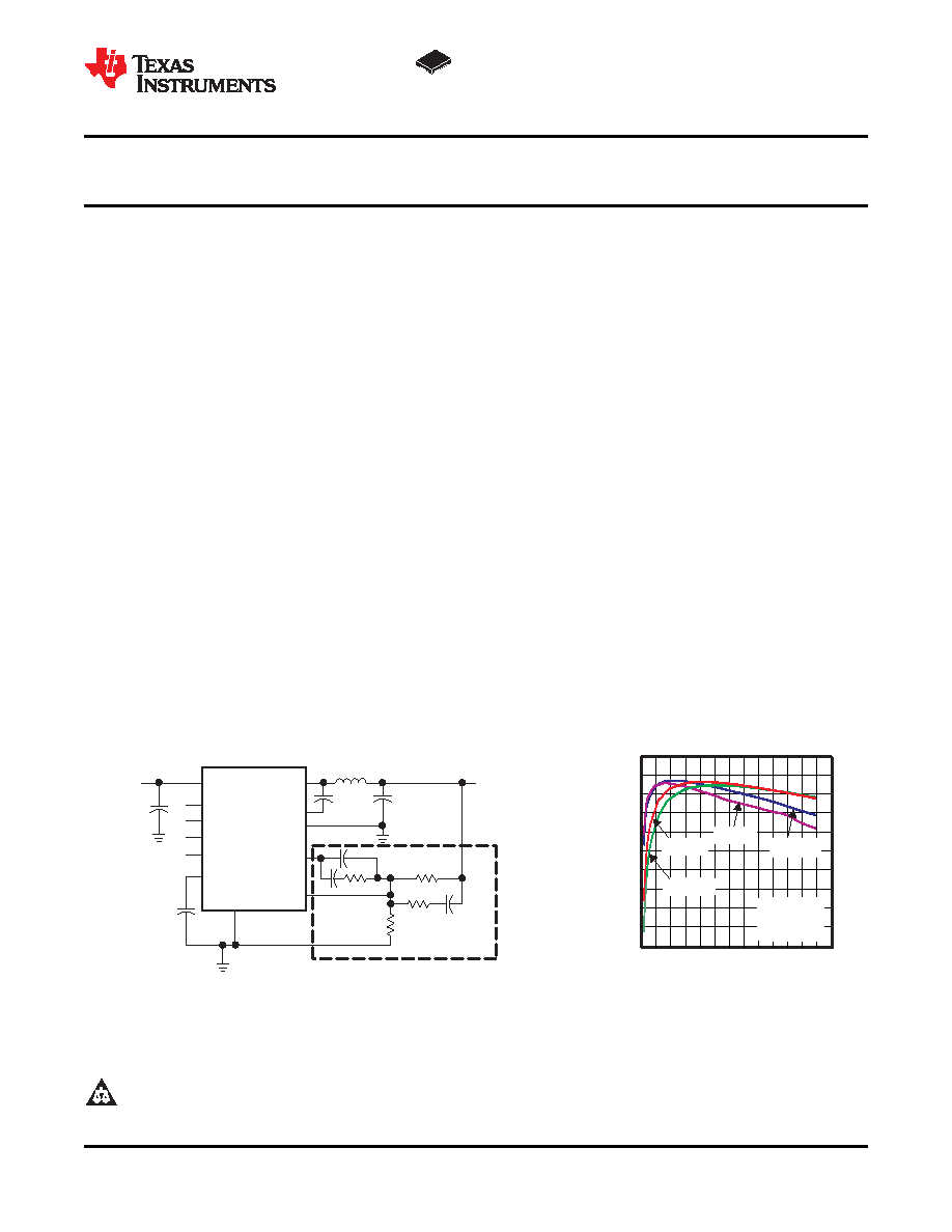
VIN
PH
BOOT
PGND
VSENSE
Output
AGND
RT
Input
TPS54617
COMP
Compensation
Network
VBIAS
SS/ENA
SYNC
PWRGD
35
41
47
53
59
65
71
77
83
89
95
Efficiency
%
EFFICIENCY vsOUTPUTCURRENT
IO OutputCurrent A
0 0.5 1 1.5 2 2.5 3 3.5 4 4.5 5 5.5 6 6.5
V =6V
I
V =5V
I
V =3V
I
V =3.3V
I
f =1600kHz
s
V =1.8V
O
www.ti.com ........................................................................................................................................... SLVS880A – NOVEMBER 2008 – REVISED JANUARY 2009
3-V TO 6-V INPUT, 6-A, SMALL SYNCHRONOUS-BUCK
SWITCHER WITH INTEGRATED FETs (SWIFT)
23
30-m MOSFET Switches for High Efficiency
at 6-A Continuous Output
As a member of the SWIFT family of dc/dc
regulators,
the
TPS54617
low-input
voltage
Adjustable Output Voltage Down to 0.9 V With
high-output
current
synchronous
buck
PWM
1% Accuracy
converter offers the same features as the TPS54610
Externally Compensated for Design Flexibility
in a small package and higher switching frequency.
Wide PWM Frequency: Fixed 350 kHz, 550 kHz,
Included on the substrate with the listed features are
or Adjustable 280 kHz to 1.6 MHz
a true, high performance, voltage error amplifier that
enables
maximum
performance
under
transient
Synchronizable to 1.6MHz
conditions and flexibility in choosing the output filter L
Load Protected by Peak Current Limit and
and C components; an undervoltage-lockout circuit to
Thermal Shutdown
prevent start-up until the input voltage reaches 3 V;
Small 3.5mm x 7mm Package and Similar
an internally and externally set slow-start circuit to
Layout to TPS54610 Reduces Board Area and
limit in-rush currents; and a power good output useful
for processor/logic reset, fault signaling, and supply
Total Cost
sequencing.
SWIFT Documentation Application Notes, and
SwitcherPro Software: www.ti.com/swift
The TPS54617 is available in a thermally enhanced
34 pin QFN (RUV) PowerPAD package, which
eliminates bulky heatsinks. TI provides evaluation
modules and the SwitcherPro design software tool
Low-Voltage, High-Density Systems With
to aid in achieving high-performance power supply
Power Distributed at 3.3 V or 5 V
designs to meet aggressive equipment development
Point of Load Regulation for High Performance
cycles.
DSPs, FPGAs, ASICs, and Microprocessors
Broadband, Networking and Optical
Communications Infrastructure
SIMPLIFIED SCHEMATIC
1
Please be aware that an important notice concerning availability, standard warranty, and use in critical applications of Texas
Instruments semiconductor products and disclaimers thereto appears at the end of this data sheet.
2
SwitcherPro, SWIFT, PowerPAD are trademarks of Texas Instruments.
3
All other trademarks are the property of their respective owners.
PRODUCTION DATA information is current as of publication date.
Copyright 2008–2009, Texas Instruments Incorporated
Products conform to specifications per the terms of the Texas
Instruments standard warranty. Production processing does not
necessarily include testing of all parameters.
相关PDF资料 |
PDF描述 |
|---|---|
| TPS54620RHLT | SWITCHING REGULATOR, 1760 kHz SWITCHING FREQ-MAX, PQCC14 |
| TPS54620RHLR | SWITCHING REGULATOR, 1760 kHz SWITCHING FREQ-MAX, PQCC14 |
| TPS54620RGYR | 11 A SWITCHING REGULATOR, 1760 kHz SWITCHING FREQ-MAX, PQCC14 |
| TPS54673PWPR | 12 A SWITCHING REGULATOR, 762 kHz SWITCHING FREQ-MAX, PDSO28 |
| TPS54673PWP | 12 A SWITCHING REGULATOR, 762 kHz SWITCHING FREQ-MAX, PDSO28 |
相关代理商/技术参数 |
参数描述 |
|---|---|
| TPS54618 | 制造商:TI 制造商全称:Texas Instruments 功能描述:2.95-V to 6-V Input, 6-A Output, 2-MHz, Synchronous Step-Down Switcher |
| TPS54618EVM-606 | 功能描述:电源管理IC开发工具 TPS54618 Eval Mod RoHS:否 制造商:Maxim Integrated 产品:Evaluation Kits 类型:Battery Management 工具用于评估:MAX17710GB 输入电压: 输出电压:1.8 V |
| TPS54618QRTERQ1 | 制造商:Texas Instruments 功能描述:IC REG BUCK SYNC ADJ 6A 16WQFN 制造商:Texas Instruments 功能描述:Synchronous Step-Down Converter |
| TPS54618RTER | 功能描述:直流/直流开关调节器 2.95-6Vin,6A,2MHz Sync Step Down SWIFT RoHS:否 制造商:International Rectifier 最大输入电压:21 V 开关频率:1.5 MHz 输出电压:0.5 V to 0.86 V 输出电流:4 A 输出端数量: 最大工作温度: 安装风格:SMD/SMT 封装 / 箱体:PQFN 4 x 5 |
| TPS54618RTET | 功能描述:直流/直流开关调节器 2.95-6Vin,6A,2MHz Sync Step Down SWIFT RoHS:否 制造商:International Rectifier 最大输入电压:21 V 开关频率:1.5 MHz 输出电压:0.5 V to 0.86 V 输出电流:4 A 输出端数量: 最大工作温度: 安装风格:SMD/SMT 封装 / 箱体:PQFN 4 x 5 |
发布紧急采购,3分钟左右您将得到回复。