- 您现在的位置:买卖IC网 > PDF目录98283 > TPS57040QDGQRQ1 (TEXAS INSTRUMENTS INC) SWITCHING REGULATOR, 2500 kHz SWITCHING FREQ-MAX, PDSO10 PDF资料下载
参数资料
| 型号: | TPS57040QDGQRQ1 |
| 厂商: | TEXAS INSTRUMENTS INC |
| 元件分类: | 稳压器 |
| 英文描述: | SWITCHING REGULATOR, 2500 kHz SWITCHING FREQ-MAX, PDSO10 |
| 封装: | GREEN, PLASTIC, MSOP-10 |
| 文件页数: | 29/51页 |
| 文件大小: | 1871K |
| 代理商: | TPS57040QDGQRQ1 |
第1页第2页第3页第4页第5页第6页第7页第8页第9页第10页第11页第12页第13页第14页第15页第16页第17页第18页第19页第20页第21页第22页第23页第24页第25页第26页第27页第28页当前第29页第30页第31页第32页第33页第34页第35页第36页第37页第38页第39页第40页第41页第42页第43页第44页第45页第46页第47页第48页第49页第50页第51页
Ioutmax
p mod =
2 ×
× Vout × Cout
p
1
z mod =
2
Resr × Cout
p
p
z
f
=
co
mod
2
sw
p
f
=
co
mod
2
f
gmps
gmea
p
=
÷
÷
è
è
co
out
ref
C
V
R4
V
1
2
f
p
=
p
C5
R4
m od
SLVSAP4A
– DECEMBER 2010 – REVISED APRIL 2011
Under Voltage Lock Out Set Point
The Under Voltage Lock Out (UVLO) can be adjusted using an external voltage divider on the EN pin of the
TPS57040-Q1. The UVLO has two thresholds, one for power up when the input voltage is rising and one for
power down or brown outs when the input voltage is falling. For the example design, the supply should turn on
and start switching once the input voltage increases above 8.9V (enabled). After the regulator starts switching, it
should continue to do so until the input voltage falls below 7.9V (UVLO stop).
The programmable UVLO and enable voltages are set using a resistor divider between Vin and ground to the EN
pin. Equation 2 through Equation 3 can be used to calculate the resistance values necessary. For the example
application, a 332k
between Vin and EN and a 56.2k between EN and ground are required to produce the 8.9
and 7.9 volt start and stop voltages.
Output Voltage and Feedback Resistors Selection
For the example design, 10.0 k
was selected for R2. Using Equation 1, R1 is calculated as 52.5 k. The
nearest standard 1% resistor is 52.3 k
. Due to current leakage of the VSENSE pin, the current flowing through
the feedback network should be greater than 1
μA in order to maintain the output voltage accuracy. This
requirement makes the maximum value of R2 equal to 800 k
. Choosing higher resistor values will decrease
quiescent current and improve efficiency at low output currents but may introduce noise immunity problems.
Compensation
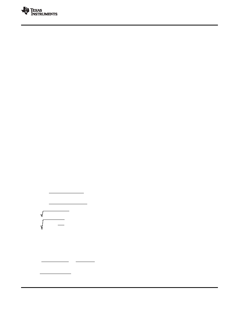
There are several methods used to compensate DC/DC regulators. The method presented here is easy to
calculate and ignores the effects of the slope compensation that is internal to the device. Since the slope
compensation is ignored, the actual cross over frequency will usually be lower than the cross over frequency
used in the calculations. This method assume the crossover frequency is between the modulator pole and the
esr zero and the esr zero is at least 10 times greater the modulator pole. Use SwitcherPro software for a more
accurate design.
To get started, the modulator pole, fpmod, and the esr zero, fz1 must be calculated using Equation 41 and
Equation 42. For Cout, use a derated value of 21.2
μf. Use equations Equation 43 and Equation 44, to estimate
a starting point for the crossover frequency, fco, to design the compensation. For the example design, fpmod is
753 Hz and fzmod is 1505 kHz. Equation 43 is the geometric mean of the modulator pole and the esr zero and
Equation 44 is the mean of modulator pole and the switching frequency. Equation 43 yields 33.7 kHz and
Equation 44 gives 16.2 kHz. Use the lower value of Equation 43 or Equation 44 for an initial crossover frequency.
For this example, fco is 16.2 kHz. Next, the compensation components are calculated. A resistor in series with a
capacitor is used to create a compensating zero. A capacitor in parallel to these two components forms the
compensating pole.
(41)
(42)
(43)
(44)
To determine the compensation resistor, R4, use Equation 45. Assume the power stage transconductance,
gmps, is 6A/V. The output voltage, Vo, reference voltage, VREF, and amplifier transconductance, gmea, are
3.3V, 0.8V and 92
μA/V, respectively. R4 is calculated to be 77.1 k, use the nearest standard value of 76.8k.
Use Equation 46 to set the compensation zero to the modulator pole frequency. Equation 46 yields 2754 pF for
compensating capacitor C5, a 2700 pF is used on the board.
(45)
(46)
Copyright
2010–2011, Texas Instruments Incorporated
35
相关PDF资料 |
PDF描述 |
|---|---|
| TPS57114QRTERQ1 | SWITCHING REGULATOR, 2000 kHz SWITCHING FREQ-MAX, PQCC16 |
| TPS60100PWP | 0.2 A SWITCHED CAPACITOR REGULATOR, 400 kHz SWITCHING FREQ-MAX, PDSO20 |
| TPS60101PWPG4 | SWITCHED CAPACITOR REGULATOR, 400 kHz SWITCHING FREQ-MAX, PDSO20 |
| TPS60101PWPRG4 | 0.1 A SWITCHED CAPACITOR REGULATOR, 400 kHz SWITCHING FREQ-MAX, PDSO20 |
| TPS60230RGTTG4 | 0.2 A SWITCHED CAPACITOR REGULATOR, 1250 kHz SWITCHING FREQ-MAX, PQCC16 |
相关代理商/技术参数 |
参数描述 |
|---|---|
| TPS57040QDRCRQ1 | 功能描述:直流/直流开关转换器 3.5-42Vin,0.5A Step Down SWIFT Cnvrtr RoHS:否 制造商:STMicroelectronics 最大输入电压:4.5 V 开关频率:1.5 MHz 输出电压:4.6 V 输出电流:250 mA 输出端数量:2 最大工作温度:+ 85 C 安装风格:SMD/SMT |
| TPS57060QDGQRQ1 | 功能描述:直流/直流开关转换器 3.5-60Vin,0.5A,2.5 MHz Step Down Cnvrtr RoHS:否 制造商:STMicroelectronics 最大输入电压:4.5 V 开关频率:1.5 MHz 输出电压:4.6 V 输出电流:250 mA 输出端数量:2 最大工作温度:+ 85 C 安装风格:SMD/SMT |
| TPS57060QDRCRQ1 | 功能描述:直流/直流开关转换器 3.5-60Vin,0.5A,2.5 MHz Step Down Cnvrtr RoHS:否 制造商:STMicroelectronics 最大输入电压:4.5 V 开关频率:1.5 MHz 输出电压:4.6 V 输出电流:250 mA 输出端数量:2 最大工作温度:+ 85 C 安装风格:SMD/SMT |
| TPS57112QRTERQ1 | 功能描述:直流/直流开关转换器 2.95-6Vin,2A,2MHz Sync St Down Cnvrtr RoHS:否 制造商:STMicroelectronics 最大输入电压:4.5 V 开关频率:1.5 MHz 输出电压:4.6 V 输出电流:250 mA 输出端数量:2 最大工作温度:+ 85 C 安装风格:SMD/SMT |
| TPS57114EVM | 制造商:Texas Instruments 功能描述:TPS57114EVM - Boxed Product (Development Kits) |
发布紧急采购,3分钟左右您将得到回复。