- 您现在的位置:买卖IC网 > PDF目录136906 > TPS61040DRVR (TEXAS INSTRUMENTS INC) 0.45 A SWITCHING REGULATOR, 1000 kHz SWITCHING FREQ-MAX, PDSO6 PDF资料下载
参数资料
| 型号: | TPS61040DRVR |
| 厂商: | TEXAS INSTRUMENTS INC |
| 元件分类: | 稳压器 |
| 英文描述: | 0.45 A SWITCHING REGULATOR, 1000 kHz SWITCHING FREQ-MAX, PDSO6 |
| 封装: | 2 X 2 MM, 0.80 MM HEIGHT, GREEN, PLASTIC, SON-6 |
| 文件页数: | 5/27页 |
| 文件大小: | 779K |
| 代理商: | TPS61040DRVR |
第1页第2页第3页第4页当前第5页第6页第7页第8页第9页第10页第11页第12页第13页第14页第15页第16页第17页第18页第19页第20页第21页第22页第23页第24页第25页第26页第27页
VIN
SW
FB
EN
GND
L1
D1
R1
R2
CFF
CO
VO
VIN
CIN
www.ti.com
SLVS413F – OCTOBER 2002 – REVISED DECEMBER 2010
INPUT CAPACITOR SELECTION
For good input voltage filtering, low ESR ceramic capacitors are recommended. A 4.7 mF ceramic input capacitor
is sufficient for most of the applications. For better input voltage filtering this value can be increased. See Table 5
and typical applications for input capacitor recommendations.
DIODE SELECTION
To achieve high efficiency a Schottky diode should be used. The current rating of the diode should meet the
peak current rating of the converter as it is calculated in the Peak Current Control section. Use the maximum
value for ILIM for this calculation. See Table 6 and the typical applications for the selection of the Schottky diode.
Table 6. Recommended Schottky Diode for Typical LCD Bias Supply (see Figure 15)
DEVICE
REVERSE VOLTAGE
COMPONENT SUPPLIER
COMMENTS
30 V
ON Semiconductor MBR0530
20 V
ON Semiconductor MBR0520
TPS61040/41
20 V
ON Semiconductor MBRM120L
High efficiency
30 V
Toshiba CRS02
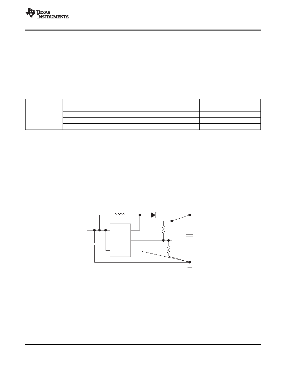
LAYOUT CONSIDERATIONS
Typical for all switching power supplies, the layout is an important step in the design; especially at high peak
currents and switching frequencies. If the layout is not carefully done, the regulator might show noise problems
and duty cycle jitter.
The input capacitor should be placed as close as possible to the input pin for good input voltage filtering. The
inductor and diode should be placed as close as possible to the switch pin to minimize the noise coupling into
other circuits. Because the feedback pin and network is a high-impedance circuit, the feedback network should
be routed away from the inductor. The feedback pin and feedback network should be shielded with a ground
plane or trace to minimize noise coupling into this circuit.
Wide traces should be used for connections in bold as shown in Figure 15. A star ground connection or ground
plane minimizes ground shifts and noise.
Figure 15. Layout Diagram
Copyright 2002–2010, Texas Instruments Incorporated
13
相关PDF资料 |
PDF描述 |
|---|---|
| TES113ZD-A8 | 1-OUTPUT 150 W DC-DC REG PWR SUPPLY MODULE |
| TC1121COA713 | SWITCHED CAPACITOR CONVERTER, 200 kHz SWITCHING FREQ-MAX, PDSO8 |
| TC54VC212ECB723 | 1-CHANNEL POWER SUPPLY SUPPORT CKT, PDSO3 |
| TC54VC3202EZB723 | 1-CHANNEL POWER SUPPLY SUPPORT CKT, PBCY3 |
| TLVH431BQDCKT | 1-OUTPUT THREE TERM VOLTAGE REFERENCE, 1.24 V, PDSO6 |
相关代理商/技术参数 |
参数描述 |
|---|---|
| TPS61040DRVRG4 | 功能描述:LED照明驱动器 28V 400-mA Sw Boost Converter RoHS:否 制造商:STMicroelectronics 输入电压:11.5 V to 23 V 工作频率: 最大电源电流:1.7 mA 输出电流: 最大工作温度: 安装风格:SMD/SMT 封装 / 箱体:SO-16N |
| TPS61040DRVT | 功能描述:LED照明驱动器 28V 400mA Sw Boost Converter RoHS:否 制造商:STMicroelectronics 输入电压:11.5 V to 23 V 工作频率: 最大电源电流:1.7 mA 输出电流: 最大工作温度: 安装风格:SMD/SMT 封装 / 箱体:SO-16N |
| TPS61040DRVTG4 | 功能描述:LED照明驱动器 28V 400-mA Sw Boost Converter RoHS:否 制造商:STMicroelectronics 输入电压:11.5 V to 23 V 工作频率: 最大电源电流:1.7 mA 输出电流: 最大工作温度: 安装风格:SMD/SMT 封装 / 箱体:SO-16N |
| TPS61040EVM-001 | 功能描述:电源管理IC开发工具 TPS61040 Boost Conv Eval Mod RoHS:否 制造商:Maxim Integrated 产品:Evaluation Kits 类型:Battery Management 工具用于评估:MAX17710GB 输入电压: 输出电压:1.8 V |
| TPS61040EVM-002 | 功能描述:电源管理IC开发工具 TPS61040 Boost Conv Eval Mod RoHS:否 制造商:Maxim Integrated 产品:Evaluation Kits 类型:Battery Management 工具用于评估:MAX17710GB 输入电压: 输出电压:1.8 V |
发布紧急采购,3分钟左右您将得到回复。