- 您现在的位置:买卖IC网 > PDF目录69517 > TPS62122DRVT (TEXAS INSTRUMENTS INC) SWITCHING REGULATOR, PDSO6 PDF资料下载
参数资料
| 型号: | TPS62122DRVT |
| 厂商: | TEXAS INSTRUMENTS INC |
| 元件分类: | 稳压器 |
| 英文描述: | SWITCHING REGULATOR, PDSO6 |
| 封装: | 2 X 2 MM, GREEN, PLASTIC, SON-6 |
| 文件页数: | 16/33页 |
| 文件大小: | 5549K |
| 代理商: | TPS62122DRVT |
第1页第2页第3页第4页第5页第6页第7页第8页第9页第10页第11页第12页第13页第14页第15页当前第16页第17页第18页第19页第20页第21页第22页第23页第24页第25页第26页第27页第28页第29页第30页第31页第32页第33页
www.ti.com
SLVSAD5 – JULY 2010
INPUT CAPACITOR SELECTION
Because of the nature of the buck converter having a pulsating input current, a low ESR input capacitor is
required for best input voltage filtering and minimizing the interference with other circuits caused by high input
voltage spikes. For most applications a 4.7F to 10F ceramic capacitor is recommended. The voltage rating
and DC bias characteristic of ceramic capacitors need to be considered. The input capacitor can be increased
without any limit for better input voltage filtering.
For specific applications like energy harvesting a tantalum or tantalum polymer capacitor can be used to achieve
a specific DC/DC converter input capacitance. Tantalum capacitors provide much better DC bias performance
compared to ceramic capacitors. In this case a 1F or 2.2F ceramic capacitor should be used in parallel to
provide low ESR.
Take care when using only small ceramic input capacitors. When a ceramic capacitor is used at the input and the
power is being supplied through long wires, such as from a wall adapter, a load step at the output or VIN step on
the input can induce large ringing at the VIN pin. This ringing can couple to the output and be mistaken as loop
instability or could even damage the part by exceeding the maximum ratings.
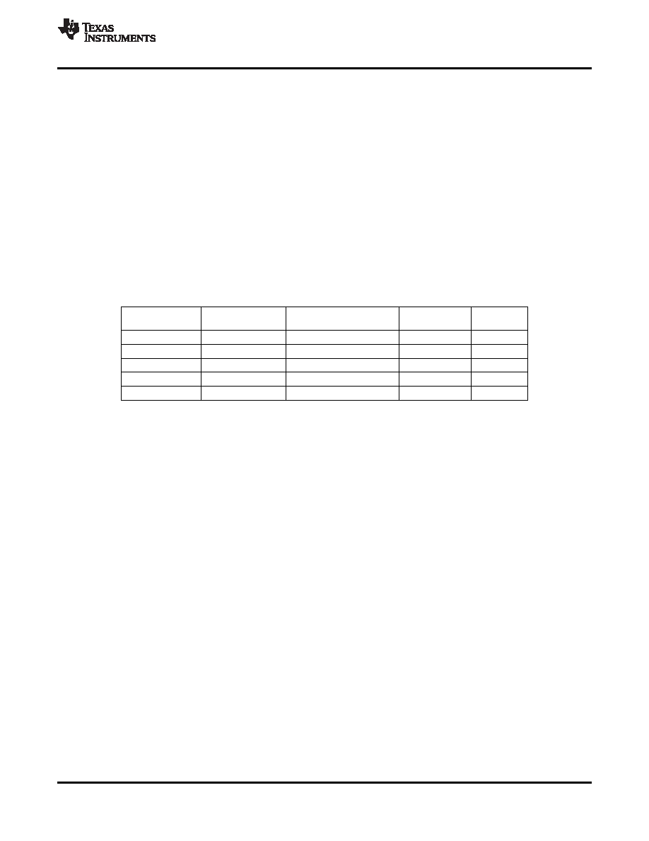
Table 3 shows a list of input/output capacitors.
Table 3. List of Capacitor
CAPACITANCE
SIZE
CAPACITOR TYPE
USAGE
SUPPLIER
[F]
4.7
0603
GRM188 series 6.3V X5R
COUT
Murata
2.2
0603
GRM188 series 6.3V X5R
COUT
Murata
4.7
0805
GRM21Bseries 25V X5R
CIN
Murata
10
0805
GRM21Bseries 16V X5R
CIN
Murata
8.2
B2(3.5 × 2.8 × 1.9)
20TQC8R2M (20V)
CIN
Sanyo
CHECKING LOOP STABILITY
The first step of circuit and stability evaluation is to look from a steady-state perspective at the following signals:
Switching node, SW
Inductor current, IL
Output ripple voltage, VO(AC)
These are the basic signals that need to be measured when evaluating a switching converter. When the
switching waveform shows large duty cycle jitter or the output voltage or inductor current shows oscillations, the
regulation loop may be unstable. This is often a result of board layout and/or L-C combination.
As a next step in the evaluation of the regulation loop, the load transient response is tested. During application of
the load transient and the turn on of the high-side MOSFET switch, the output capacitor must supply all of the
current required by the load. VOUT immediately shifts by an amount equal to ΔI(LOAD) × ESR, where ESR is the
effective series resistance of COUT. ΔI(LOAD) begins to charge or discharge COUT generating a feedback error
signal used by the regulator to return VOUT to its steady-state value. The results are most easily interpreted when
the device operates in PWM mode.
During this recovery time, VOUT can be monitored for settling time, overshoot or ringing that helps judge the
converter’s stability. Without any ringing, the loop has usually more than 45° of phase margin. Because the
damping factor of the circuitry is directly related to several resistive parameters (e.g., MOSFET RDS(on)) which are
temperature dependent, the loop stability analysis should be done over the input voltage range, load current
range, and temperature range
LAYOUT CONSIDERATIONS
As for all switching power supplies, the layout is an important step in the design. Proper function of the device
demands careful attention to PCB layout. Care must be taken in board layout to get the specified performance. If
the layout is not carefully done, the regulator could show poor line and/or load regulation, stability issues as well
as EMI problems. It is critical to provide a low inductance, impedance ground path. Therefore, use wide and
short traces for the main current paths. The input capacitor should be placed as close as possible to the IC pins
as well as the inductor and output capacitor.
Copyright 2010, Texas Instruments Incorporated
23
相关PDF资料 |
PDF描述 |
|---|---|
| TPS62201DBVTG4 | 0.67 A SWITCHING REGULATOR, 1500 kHz SWITCHING FREQ-MAX, PDSO5 |
| TPS62201DBVRG4 | 0.67 A SWITCHING REGULATOR, 1500 kHz SWITCHING FREQ-MAX, PDSO5 |
| TPS62203DBVRG4 | 0.67 A SWITCHING REGULATOR, 1500 kHz SWITCHING FREQ-MAX, PDSO5 |
| TPS62208DBVT | 0.67 A SWITCHING REGULATOR, 1500 kHz SWITCHING FREQ-MAX, PDSO5 |
| TPS62203DBVTG4 | 0.67 A SWITCHING REGULATOR, 1500 kHz SWITCHING FREQ-MAX, PDSO5 |
相关代理商/技术参数 |
参数描述 |
|---|---|
| TPS62122DRVT | 制造商:Texas Instruments 功能描述:IC SYNC BUCK DC/DC CONTROLLER 800KHZ 制造商:Texas Instruments 功能描述:IC, SYNC BUCK DC/DC CONTROLLER, 800KHZ, 6-SON |
| TPS62122EVM-586 | 功能描述:电源管理IC开发工具 TPS62122 Eval Mod RoHS:否 制造商:Maxim Integrated 产品:Evaluation Kits 类型:Battery Management 工具用于评估:MAX17710GB 输入电压: 输出电压:1.8 V |
| TPS62122EVM-586 | 制造商:Texas Instruments 功能描述:EVAL BOARD, TPS62122, BUCK CONVERTER |
| TPS62125DSGR | 功能描述:开关变换器、稳压器与控制器 3V-17V, 300mA Buck Converter RoHS:否 制造商:Texas Instruments 输出电压:1.2 V to 10 V 输出电流:300 mA 输出功率: 输入电压:3 V to 17 V 开关频率:1 MHz 工作温度范围: 安装风格:SMD/SMT 封装 / 箱体:WSON-8 封装:Reel |
| TPS62125DSGT | 功能描述:开关变换器、稳压器与控制器 3V-17V, 300mA Buck Converter RoHS:否 制造商:Texas Instruments 输出电压:1.2 V to 10 V 输出电流:300 mA 输出功率: 输入电压:3 V to 17 V 开关频率:1 MHz 工作温度范围: 安装风格:SMD/SMT 封装 / 箱体:WSON-8 封装:Reel |
发布紧急采购,3分钟左右您将得到回复。