- 您现在的位置:买卖IC网 > PDF目录225340 > TPS70702PWP (Texas Instruments, Inc.) DUAL-OUTPUT LOW-DROPOUT VOLTAGE REGULATORS WITH POWER UP SEQUENCING FOR SPLIT VOLTAGE DSP SYSTEMS PDF资料下载
参数资料
| 型号: | TPS70702PWP |
| 厂商: | Texas Instruments, Inc. |
| 元件分类: | 线性稳压 |
| 英文描述: | DUAL-OUTPUT LOW-DROPOUT VOLTAGE REGULATORS WITH POWER UP SEQUENCING FOR SPLIT VOLTAGE DSP SYSTEMS |
| 中文描述: | 两用低压差最多可劈开电压DSP系统序列电源电压稳压器的输出 |
| 文件页数: | 31/34页 |
| 文件大小: | 505K |
| 代理商: | TPS70702PWP |
第1页第2页第3页第4页第5页第6页第7页第8页第9页第10页第11页第12页第13页第14页第15页第16页第17页第18页第19页第20页第21页第22页第23页第24页第25页第26页第27页第28页第29页第30页当前第31页第32页第33页第34页
TPS70745, TPS70748, TPS70751, TPS70758, TPS70702
DUAL-OUTPUT LOW-DROPOUT VOLTAGE REGULATORS
WITH POWER UP SEQUENCING FOR SPLIT VOLTAGE DSP SYSTEMS
SLVS291 – MAY 2000
6
POST OFFICE BOX 655303
DALLAS, TEXAS 75265
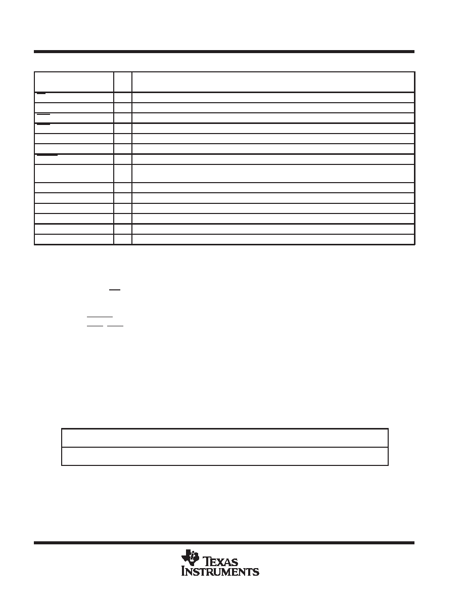
Terminal Functions
TERMINAL
I/O
DESCRIPTION
NAME
NO.
I/O
DESCRIPTION
EN
6
I
Active low enable
GND
8
Ground
MR1
4
I
Manual reset input 1, active low, pulled up internally
MR2
5
I
Manual reset input 2, active low, pulled up internally
NC
1, 11, 20
No connection
PG1
16
O
Open drain output, low when VOUT1 voltage is less than 95% of the nominal regulated voltage
RESET
15
O
Open drain output, SVS (power on reset) signal, active low
SEQ
7
I
Power up sequence control: SEQ=High, VOUT2 powers up first; SEQ=Low, VOUT1 powers up first, SEQ
terminal pulled up internally.
VIN1
2, 3
I
Input voltage of regulator 1
VIN2
9, 10
I
Input voltage of regulator 2
VOUT1
18, 19
O
Output voltage of regulator 1
VOUT2
12, 13
O
Output voltage of regulator 2
VSENSE2/FB2
14
I
Regulator 2 output voltage sense/ regulator 2 feedback for adjustable
VSENSE1/FB1
17
I
Regulator 1 output voltage sense/ regulator 1 feedback for adjustable
absolute maximum ratings over operating junction temperature (unless otherwise noted)
Input voltage range:VIN1
– 0.3 V to 7 V
. . . . . . . . . . . . . . . . . . . . . . . . . . . . . . . . . . . . . . . . . . . . . . . . . . . . . . . . . .
VIN2
– 0.3 V to 7 V
. . . . . . . . . . . . . . . . . . . . . . . . . . . . . . . . . . . . . . . . . . . . . . . . . . . . . . . . . .
Voltage range at EN
– 0.3 V to 7 V
. . . . . . . . . . . . . . . . . . . . . . . . . . . . . . . . . . . . . . . . . . . . . . . . . . . . . . . . . . . . . . . .
Output voltage range (VOUT1, VSENSE1)
5.5 V
. . . . . . . . . . . . . . . . . . . . . . . . . . . . . . . . . . . . . . . . . . . . . . . . . . . .
Output voltage range (VOUT2, VSENSE2)
5.5 V
. . . . . . . . . . . . . . . . . . . . . . . . . . . . . . . . . . . . . . . . . . . . . . . . . . . .
Maximum RESET, PG1 voltage
7 V
. . . . . . . . . . . . . . . . . . . . . . . . . . . . . . . . . . . . . . . . . . . . . . . . . . . . . . . . . . . . . . .
Maximum MR1, MR2, and SEQ voltage
VIN1
. . . . . . . . . . . . . . . . . . . . . . . . . . . . . . . . . . . . . . . . . . . . . . . . . . . . . . .
Peak output current
Internally limited
. . . . . . . . . . . . . . . . . . . . . . . . . . . . . . . . . . . . . . . . . . . . . . . . . . . . . . . . . . . . . .
Continuous total power dissipation
See Dissipation Rating Tables
. . . . . . . . . . . . . . . . . . . . . . . . . . . . . . . . . . . .
Operating virtual junction temperature range, TJ
–40
°C to 125°C
. . . . . . . . . . . . . . . . . . . . . . . . . . . . . . . . . . . . .
Storage temperature range, Tstg
–65
°C to 150°C
. . . . . . . . . . . . . . . . . . . . . . . . . . . . . . . . . . . . . . . . . . . . . . . . . . .
ESD rating, HBM
2 kV
. . . . . . . . . . . . . . . . . . . . . . . . . . . . . . . . . . . . . . . . . . . . . . . . . . . . . . . . . . . . . . . . . . . . . . . . . .
Stresses beyond those listed under “absolute maximum ratings” may cause permanent damage to the device. These are stress ratings only, and
functional operation of the device at these or any other conditions beyond those indicated under “recommended operating conditions” is not
implied. Exposure to absolute-maximum-rated conditions for extended periods may affect device reliability.
All voltages are tied to network ground.
DISSIPATION RATING TABLE
PACKAGE
AIR FLOW
(CFM)
TA ≤ 25°C
DERATING FACTOR
TA = 70°C
TA = 85°C
PWP§
0
3.067 W
30.67 mW/
°C
1.687 W
1.227 W
PWP§
250
4.115 W
41.15 mW/
°C
2.265 W
1.646 W
§ This parameter is measured with the recommended copper heat sink pattern on a 4-layer PCB, 1 oz. copper on 4-in
× 4-in
ground layer. For more information, refer to TI technical brief SLMA002.
相关PDF资料 |
PDF描述 |
|---|---|
| TPS70745PWP | DUAL-OUTPUT LOW-DROPOUT VOLTAGE REGULATORS WITH POWER UP SEQUENCING FOR SPLIT VOLTAGE DSP SYSTEMS |
| TPS70751PWP | DUAL-OUTPUT LOW-DROPOUT VOLTAGE REGULATORS WITH POWER UP SEQUENCING FOR SPLIT VOLTAGE DSP SYSTEMS |
| TPS70758PWPRG4 | 2-CHANNEL POWER SUPPLY SUPPORT CKT, PDSO20 |
| TPS70802PWP | DUAL-OUTPUT LOW-DROPOUT VOLTAGE REGULATORS WITH INTEGRATED SVS FOR SPLIT VOLTAGE SYSTEMS |
| TPS70845PWP | DUAL-OUTPUT LOW-DROPOUT VOLTAGE REGULATORS WITH INTEGRATED SVS FOR SPLIT VOLTAGE SYSTEMS |
相关代理商/技术参数 |
参数描述 |
|---|---|
| TPS70702PWPG4 | 功能描述:低压差稳压器 - LDO Dual Adj 1A/2A LDO RoHS:否 制造商:Texas Instruments 最大输入电压:36 V 输出电压:1.4 V to 20.5 V 回动电压(最大值):307 mV 输出电流:1 A 负载调节:0.3 % 输出端数量: 输出类型:Fixed 最大工作温度:+ 125 C 安装风格:SMD/SMT 封装 / 箱体:VQFN-20 |
| TPS70702PWPR | 功能描述:低压差稳压器 - LDO Dual-Output LDO RoHS:否 制造商:Texas Instruments 最大输入电压:36 V 输出电压:1.4 V to 20.5 V 回动电压(最大值):307 mV 输出电流:1 A 负载调节:0.3 % 输出端数量: 输出类型:Fixed 最大工作温度:+ 125 C 安装风格:SMD/SMT 封装 / 箱体:VQFN-20 |
| TPS70702PWPRG4 | 功能描述:低压差稳压器 - LDO Dual-Output LDO RoHS:否 制造商:Texas Instruments 最大输入电压:36 V 输出电压:1.4 V to 20.5 V 回动电压(最大值):307 mV 输出电流:1 A 负载调节:0.3 % 输出端数量: 输出类型:Fixed 最大工作温度:+ 125 C 安装风格:SMD/SMT 封装 / 箱体:VQFN-20 |
| TPS70745 | 制造商:TI 制造商全称:Texas Instruments 功能描述:DUAL-OUTPUT LOW-DROPOUT VOLTAGE REGULATORS WITH POWER UP SEQUENCING FOR SPLIT VOLTAGE DSP SYSTEMS |
| TPS70745PWP | 功能描述:低压差稳压器 - LDO 3.3V/1.2V 250/125mA RoHS:否 制造商:Texas Instruments 最大输入电压:36 V 输出电压:1.4 V to 20.5 V 回动电压(最大值):307 mV 输出电流:1 A 负载调节:0.3 % 输出端数量: 输出类型:Fixed 最大工作温度:+ 125 C 安装风格:SMD/SMT 封装 / 箱体:VQFN-20 |
发布紧急采购,3分钟左右您将得到回复。