- 您现在的位置:买卖IC网 > PDF目录272328 > TS80C51BH (INTEL CORP) 8-BIT, MROM, 12 MHz, MICROCONTROLLER, PQFP44 PDF资料下载
参数资料
| 型号: | TS80C51BH |
| 厂商: | INTEL CORP |
| 元件分类: | 微控制器/微处理器 |
| 英文描述: | 8-BIT, MROM, 12 MHz, MICROCONTROLLER, PQFP44 |
| 封装: | QFP-44 |
| 文件页数: | 4/21页 |
| 文件大小: | 2233K |
| 代理商: | TS80C51BH |
87C51/80C51BH/80C31BH
EXPLANATION OF THE AC SYMBOLS
Each timing symbol has 5 characters. The first char-
acter is always a `T' (stands for time). The other
characters, depending on their positions, stand for
the name of a signal or the logical status of that
signal. The following is a list of all the characters and
what they stand for.
A:Address.
C:Clock.
D:Input data.
H:Logic level HIGH.
I:Instruction (program memory contents).
L:Logic level LOW, or ALE.
P:PSEN.
Q:Output data.
R:RD signal.
T:Time.
V:Valid.
W:WR signal.
X:No longer a valid logic level.
Z:Float.
For example,
TAVLL e Time from Address Valid to ALE Low.
TLLPL e Time from ALE Low to PSEN Low.
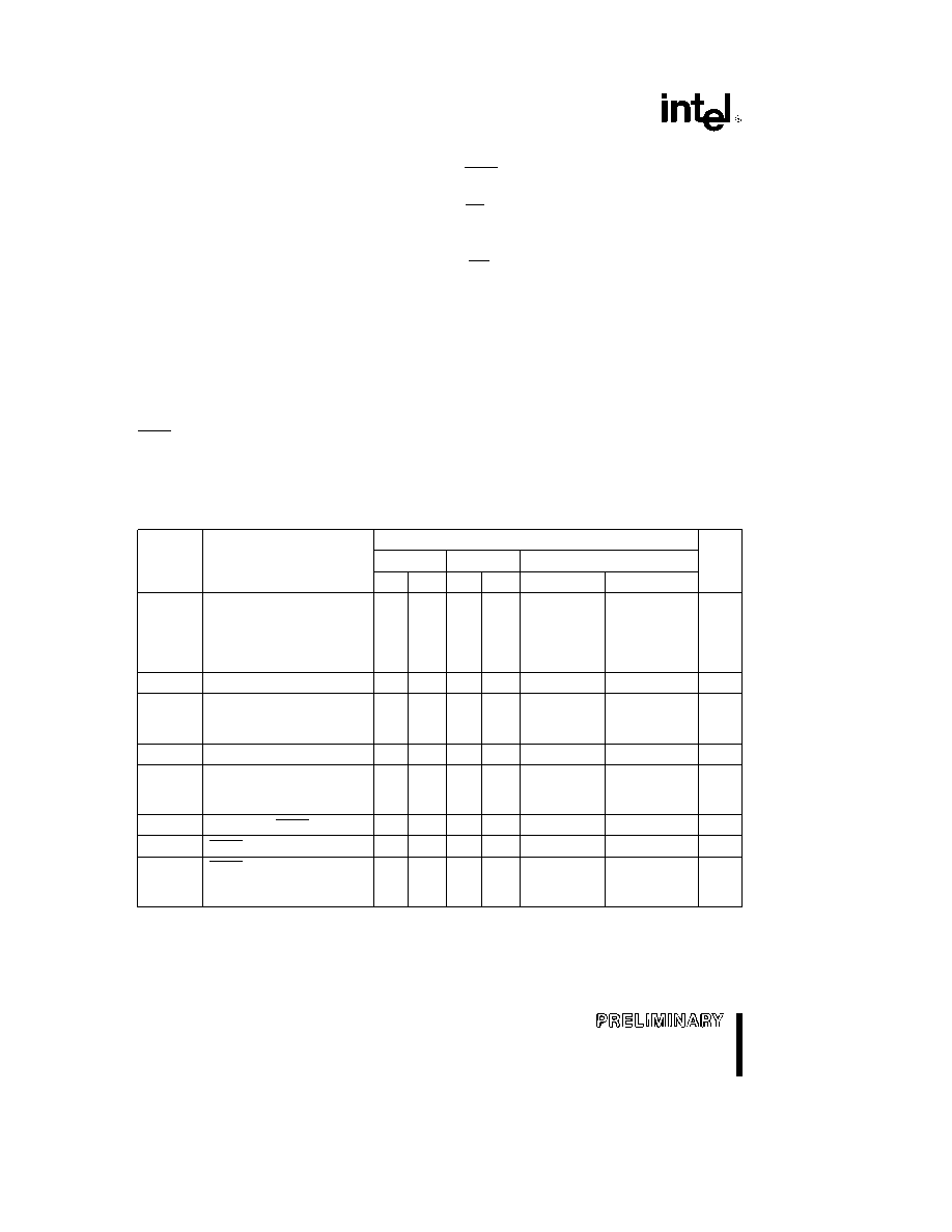
AC CHARACTERISTICS
: (Over Operating Conditions; Load Capacitance for Port 0, ALE, and
PSEN e 100 pF; Load Capacitance for All Other Outputs e 80 pF)
EXTERNAL MEMORY CHARACTERISTICS
All parameter values apply to all devices unless otherwise indicated. In this table, 87C51/BH refers to
87C51/BH, 87C51-1/BH-1 and 87C51-2/BH-2.
Symbol
Parameter
Oscillator
Units
12 MHz
24 MHz
Variable
Min
Max
Min
Max
Min
Max
1/TCLCL Oscillator Frequency
87C51/BH
3.5
12
MHz
87C51-1/BH-1
3.5
16
MHz
87C51-2/BH-2
0.5
12
MHz
87C51-24/BH-24
3.5
24
MHz
TLHLL
ALE Pulse Width
127
43
2TCLCLb40
ns
TAVLL
Address Valid to ALE Low
87C51/BH
43
TCLCLb40
ns
87C51-24/BH-24
12
TCLCLb30
ns
TLLAX
Address Hold After ALE Low
53
12
TCLCLb30
ns
TLLIV
ALE Low to Valid Instr In
87C51/BH
234
4TCLCLb100
ns
87C51-24/BH-24
91
4TCLCLb75
ns
TLLPL
ALE Low to PSEN Low
53
12
TCLCLb30
ns
TPLPH
PSEN Pulse Width
205
80
3TCLCLb45
ns
TPLIV
PSEN Low to Valid Instr In
87C51/BH
145
3TCLCLb105
ns
87C51-24/BH-24
35
3TCLCLb90
ns
12
相关PDF资料 |
PDF描述 |
|---|---|
| TSC80C31-30CXB | 8-BIT, 30 MHz, MICROCONTROLLER, UUC40 |
| T83C154DXXX-20 | 8-BIT, MROM, 20 MHz, MICROCONTROLLER, PQFP44 |
| TA80486DX2-50 | 32-BIT, 50 MHz, MICROPROCESSOR, CPGA168 |
| T80C32U-S:D | 8-BIT, 20 MHz, MICROCONTROLLER, PQFP44 |
| T83C154DUFXXX-30:R | 8-BIT, MROM, 30 MHz, MICROCONTROLLER, PQFP44 |
相关代理商/技术参数 |
参数描述 |
|---|---|
| TS80C51BH-1 | 制造商:未知厂家 制造商全称:未知厂家 功能描述:8-Bit Microcontroller |
| TS80C51BH-2 | 制造商:未知厂家 制造商全称:未知厂家 功能描述:8-Bit Microcontroller |
| TS80C51BH-24 | 制造商:未知厂家 制造商全称:未知厂家 功能描述:8-Bit Microcontroller |
| TS80C51BHP | 制造商:未知厂家 制造商全称:未知厂家 功能描述:8-Bit Microcontroller |
| TS80C51BHP-1 | 制造商:未知厂家 制造商全称:未知厂家 功能描述:8-Bit Microcontroller |
发布紧急采购,3分钟左右您将得到回复。