- 您现在的位置:买卖IC网 > PDF目录98301 > TSA1005I-40IF (STMICROELECTRONICS) 2-CH 10-BIT PROPRIETARY METHOD ADC, PARALLEL ACCESS, PQFP48 PDF资料下载
参数资料
| 型号: | TSA1005I-40IF |
| 厂商: | STMICROELECTRONICS |
| 元件分类: | ADC |
| 英文描述: | 2-CH 10-BIT PROPRIETARY METHOD ADC, PARALLEL ACCESS, PQFP48 |
| 封装: | 7 X 7 MM, TQFP-48 |
| 文件页数: | 7/22页 |
| 文件大小: | 540K |
| 代理商: | TSA1005I-40IF |
Obsolete
Product(s)
- Obsolete
Product(s)
TSA1005
15/22
NO
T
FOR
NEW
DESI
G
N
External reference and common mode
Each of the voltages VREFP and INCM can be
fixed externally to better fit to the application
needs
(Refer
to
table
íOPERATING
CONDITIONSí page 4 for min/max values).
The VREFP, VREFM voltages set the analog
dynamic at the input of the converter that has a full
scale amplitude of 2*(VREFP-VREFM). Using
internal references, the dynamic range is 1.8V.
The INCM is the mid voltage of the analog input
signal.
It is possible to use an external reference voltage
device for specific applications requiring even
better
linearity,
accuracy
or
enhanced
temperature behavior.
Using
the
STMicroelectronics
TS821
or
TS4041-1.2 Vref leads to optimum performances
when configured as shown on Figure 2.
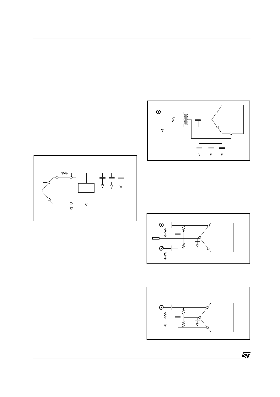
Figure 2: External reference setting
DRIVING THE DIFFERENTIAL ANALOG
INPUTS
The TSA1005 has been designed to obtain
optimum performances when being differentially
driven. An RF transformer is a good way to
achieve such performances.
Figure 3 describes the schematics. The input
signal is fed to the primary of the transformer,
while the secondary drives both ADC inputs. The
common mode voltage of the ADC (INCM) is
connected to the center-tap of the secondary of
the transformer in order to bias the input signal
around this common voltage, internally set to
0.46V. It determines the DC component of the
analog signal. As being an high impedance input,
it acts as an I/O and can be externally driven to
adjust
this
DC
component.
The
INCM
is
decoupled to maintain a low noise level on this
node. Our evaluation board is mounted with a 1:1
ADT1-1WT transformer from Minicircuits. You
might also use a higher impedance ratio (1:2 or
1:4) to reduce the driving requirement on the
analog signal source.
Each analog input can drive a 1.4Vpp amplitude
input signal, so the resultant differential amplitude
is 2.8Vpp.
Figure 3: Differential input configuration with
transformer
Figure 4 represents the biasing of a differential
input signal in AC-coupled differential input
configuration. Both inputs VIN and VINB are
centered around the common mode voltage, that
can be let internal or fixed externally.
Figure 4: AC-coupled differential input
Figure 5: AC-coupled Single-ended input
1k
TSA1005
VIN
VINB
VREFM
VREFP
external
reference
VCCA
330pF
4.7uF
10nF
TS821
TS4041
TSA1005
VIN
VINB
INCM
50
33pF
330pF
470nF
10nF
Analog source
1:1
ADT1-1
I or Q ch.
50
10nF
TSA1005
VIN
VINB
INCM
33pF
100k
100k
50
10nF
common
mode
50
10nF
Signal source
TSA1005
VIN
VINB
INCM
33pF
100k
100k
相关PDF资料 |
PDF描述 |
|---|---|
| TSA1005-20IF | 2-CH 10-BIT PROPRIETARY METHOD ADC, PARALLEL ACCESS, PQFP48 |
| TSA1005-40IF | 2-CH 10-BIT PROPRIETARY METHOD ADC, PARALLEL ACCESS, PQFP48 |
| TSA1041IFT | 4-CH 10-BIT PROPRIETARY METHOD ADC, PARALLEL ACCESS, PQFP48 |
| TSA1041IF | 4-CH 10-BIT PROPRIETARY METHOD ADC, PARALLEL ACCESS, PQFP48 |
| TSA1201IF | 1-CH 12-BIT PROPRIETARY METHOD ADC, PARALLEL ACCESS, PQFP48 |
相关代理商/技术参数 |
参数描述 |
|---|---|
| TSA1015 | 制造商:未知厂家 制造商全称:未知厂家 功能描述:PNP SILICON TRANSISTOR |
| TSA1036 | 制造商:TSC 制造商全称:Taiwan Semiconductor Company, Ltd 功能描述:General Purpose PNP Transistor |
| TSA1036CX | 功能描述:两极晶体管 - BJT PNP Transistor RoHS:否 制造商:STMicroelectronics 配置: 晶体管极性:PNP 集电极—基极电压 VCBO: 集电极—发射极最大电压 VCEO:- 40 V 发射极 - 基极电压 VEBO:- 6 V 集电极—射极饱和电压: 最大直流电集电极电流: 增益带宽产品fT: 直流集电极/Base Gain hfe Min:100 A 最大工作温度: 安装风格:SMD/SMT 封装 / 箱体:PowerFLAT 2 x 2 |
| TSA1036CX RF | 制造商:SKMI/Taiwan 功能描述:SOT-23;PNP TRANSISTOR |
| TSA1036CXRF | 制造商:TSC 制造商全称:Taiwan Semiconductor Company, Ltd 功能描述:General Purpose PNP Transistor |
发布紧急采购,3分钟左右您将得到回复。