参数资料
| 型号: | UCC28250RGPT |
| 厂商: | Texas Instruments |
| 文件页数: | 17/53页 |
| 文件大小: | 0K |
| 描述: | IC REG CTRLR PWM CM/VM 20-QFN |
| 标准包装: | 1 |
| PWM 型: | 电流/电压模式 |
| 输出数: | 1 |
| 频率 - 最大: | 1MHz |
| 占空比: | 100% |
| 电源电压: | 4.7 V ~ 17 V |
| 降压: | 无 |
| 升压: | 无 |
| 回扫: | 无 |
| 反相: | 无 |
| 倍增器: | 无 |
| 除法器: | 无 |
| Cuk: | 无 |
| 隔离: | 无 |
| 工作温度: | -40°C ~ 125°C |
| 封装/外壳: | 20-VFQFN 裸露焊盘 |
| 包装: | 标准包装 |
| 其它名称: | 296-27777-6 |
第1页第2页第3页第4页第5页第6页第7页第8页第9页第10页第11页第12页第13页第14页第15页第16页当前第17页第18页第19页第20页第21页第22页第23页第24页第25页第26页第27页第28页第29页第30页第31页第32页第33页第34页第35页第36页第37页第38页第39页第40页第41页第42页第43页第44页第45页第46页第47页第48页第49页第50页第51页第52页第53页
�� ���
���
���SLUSA29C� –� APRIL� 2010� –� REVISED� JULY� 2011�
�RAMP/CS� (PWM� Ramp� Input� or� Current� Sense� Input)� (16/3)�
�The� UCC28250� can� be� controlled� using� either� voltage� mode� or� current� mode.� RAMP/CS� is� a� multi-function� pin�
�used� either� to� generate� the� ramp� signal� for� voltage� mode� control� or� to� sense� current� for� current� mode� control.The�
�following� sections� describe� the� RAMP/CS� functionality� for� voltage� mode� and� current� mode� control.�
�RAMP:� Voltage� Mode� Control� with� Feed-Forward� Operation�
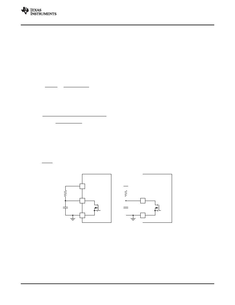
�For� voltage� mode� control,� a� resistor� R� CS� and� a� capacitor� C� CS� must� be� connected� to� the� RAMP/CS� pin� as� shown�
�in� Figure� 11� .� The� internal� pull-down� switch� has� approximately� 40-� Ω� on-resistance.� The� RAMP/CS� pin� is� clamped�
�internally� to� 4� V� for� internal� device� protection.� The� C� CS� value� must� be� small� enough� to� discharge� the� RAMP/CS�
�pin� from� its� peak� voltage� to� ground� within� the� pulse� width� of� the� BLANK� signal� (T� D(sp)� +� 70� ns).� The� following�
�formula� derives� a� C� CS� value.�
�C� CS� <� ?� ÷� ′� d(SP)�
�40� W�
�è� ?�
�?4V/2? T +70ns�
�4V�
�(4)�
�A� C� CS� value� less� than� 650� pF� works� for� most� applications.� In� order� to� minimize� the� impacts� of� parasitic�
�capacitance� caused� by� the� PCB� layout� and� routing,� a� minimum� of� 100� pF� is� recommended� for� C� CS� .� Once� C� CS� is�
�determined,� R� CS� can� be� calculated� according� to� the� desired� ramp� peak� amplitude.�
�è� V� CHARGE� PK�
�2� ′� ln� ?�
�R� CS� =�
�?� V� CHARGE�
�1�
�-� V�
�?�
�÷� ′� C� CS� ′� f� SW�
�?�
�(5)�
�In� this� equation,� the� V� CHARGE� is� the� voltage� used� to� generate� the� ramp,� V� PK� is� the� desired� ramp� amplitude� and�
�the� f� SW� is� the� switching� frequency.�
�Choose� the� ramp� amplitude� to� accommodate� the� voltage� range� of� the� COMP� pin� and� the� maximum� duty� cycle�
�required� by� the� power� stage.� Use� the� following� equation� to� select� V� PK� ,� in� the� equation,� D� MAX� is� the� maximum� duty�
�cycle� for� primary� outputs.�
�V� PK� =�
�1.4 V�
�D� MAX�
�R� CS�
�UCC28250�
�VREF�
�RAMP/CS�
�V� IN� 36� V� to� 75� V�
�R� CS�
�UCC28250�
�RAMP/CS�
�(6)�
�C� CS�
�GND�
�BLANK�
�C� CS�
�GND�
�BLANK�
�Figure� 11.� Fixed� Ramp� Generation/Ramp� Generation� With� Input� Voltage� Feedforward�
�Voltage� feed-forward� can� be� achieved� by� driving� R� CS� from� line� input� VIN.� The� peak� of� RAMP/CS� is� proportional�
�to� VIN� and� output� has� have� much� faster� line� transient� response.� When� the� UCC28250� is� used� for� the�
�primary-side� control,� RAMP� parameters� are� critical� for� the� optimal� pre-biased� start� up� performance.� Refer� to� the�
�‘� Voltage� Mode� Control� and� Input� Voltage� Feed-Forward� ’� section� of� the� Functional� Description� section� for� a�
�detailed� design� procedure� of� choosing� R� CS� .�
�If� the� line� input� cannot� be� easily� accessed� due� to� limited� board� area� or� other� limitation,� a� RAMP� signal� with� fixed�
�peak� voltage� can� be� implemented� by� simply� driving� R� CS� from� 3.3� V� VREF� (� Figure� 11� ).�
�Copyright� ?� 2010� –� 2011,� Texas� Instruments� Incorporated�
�Product� Folder� Link(s):� UCC28250�
��17�
�相关PDF资料 |
PDF描述 |
|---|---|
| MCP1804T-C002I/OT | IC REG LDO 12V .15A SOT23-5 |
| GCC50DRTH | CONN EDGECARD 100PS DIP .100 SLD |
| GSC25DRAN | CONN EDGECARD 50POS R/A .100 SLD |
| RSC26DRAS | CONN EDGECARD 52POS R/A .100 SLD |
| UPM1V271MPD | CAP ALUM 270UF 35V 20% RADIAL |
相关代理商/技术参数 |
参数描述 |
|---|---|
| UCC28250RGPT | 制造商:Texas Instruments 功能描述:PWM CONTROLLER IC 17V QFN-20 制造商:Texas Instruments 功能描述:IC, PWM CONTROLLER, 17V, QFN-20 |
| UCC28251 | 制造商:TI 制造商全称:Texas Instruments 功能描述:Advanced PWM Controller With Pre-Bias Operation |
| UCC28251PW | 功能描述:电压模式 PWM 控制器 Advanced PWM Cntlr RoHS:否 制造商:Texas Instruments 输出端数量:1 拓扑结构:Buck 输出电压:34 V 输出电流: 开关频率: 工作电源电压:4.5 V to 5.5 V 电源电流:600 uA 最大工作温度:+ 125 C 最小工作温度:- 40 C 封装 / 箱体:WSON-8 封装:Reel |
| UCC28251PWR | 功能描述:电压模式 PWM 控制器 Advanced PWM Cntlr RoHS:否 制造商:Texas Instruments 输出端数量:1 拓扑结构:Buck 输出电压:34 V 输出电流: 开关频率: 工作电源电压:4.5 V to 5.5 V 电源电流:600 uA 最大工作温度:+ 125 C 最小工作温度:- 40 C 封装 / 箱体:WSON-8 封装:Reel |
| UCC28251PWT | 制造商:TI 制造商全称:Texas Instruments 功能描述:Advanced PWM Controller With Pre-Bias Operation |
发布紧急采购,3分钟左右您将得到回复。