- 您现在的位置:买卖IC网 > PDF目录15401 > UCC2891PW (Texas Instruments)IC PWM CNTRLR CLAMP P-CH 16TSSOP PDF资料下载
参数资料
| 型号: | UCC2891PW |
| 厂商: | Texas Instruments |
| 文件页数: | 7/41页 |
| 文件大小: | 0K |
| 描述: | IC PWM CNTRLR CLAMP P-CH 16TSSOP |
| 产品培训模块: | 120V High-Side/Low-Side MOSFET Driver (UCC27200) |
| 标准包装: | 90 |
| PWM 型: | 电流模式 |
| 输出数: | 1 |
| 频率 - 最大: | 1MHz |
| 占空比: | 73% |
| 电源电压: | 8.5 V ~ 16 V |
| 降压: | 无 |
| 升压: | 无 |
| 回扫: | 是 |
| 反相: | 无 |
| 倍增器: | 无 |
| 除法器: | 无 |
| Cuk: | 无 |
| 隔离: | 是 |
| 工作温度: | -40°C ~ 125°C |
| 封装/外壳: | 16-TSSOP(0.173",4.40mm 宽) |
| 包装: | 管件 |
| 其它名称: | 296-17240 296-17240-5 296-17240-ND |
第1页第2页第3页第4页第5页第6页当前第7页第8页第9页第10页第11页第12页第13页第14页第15页第16页第17页第18页第19页第20页第21页第22页第23页第24页第25页第26页第27页第28页第29页第30页第31页第32页第33页第34页第35页第36页第37页第38页第39页第40页第41页
�� �
�
�UCC2891,� UCC2892�
�UCC2893,� UCC2894�
�SLUS542F� ?� OCTOBER� 2003� ?� REVISED� JULY� 2009�
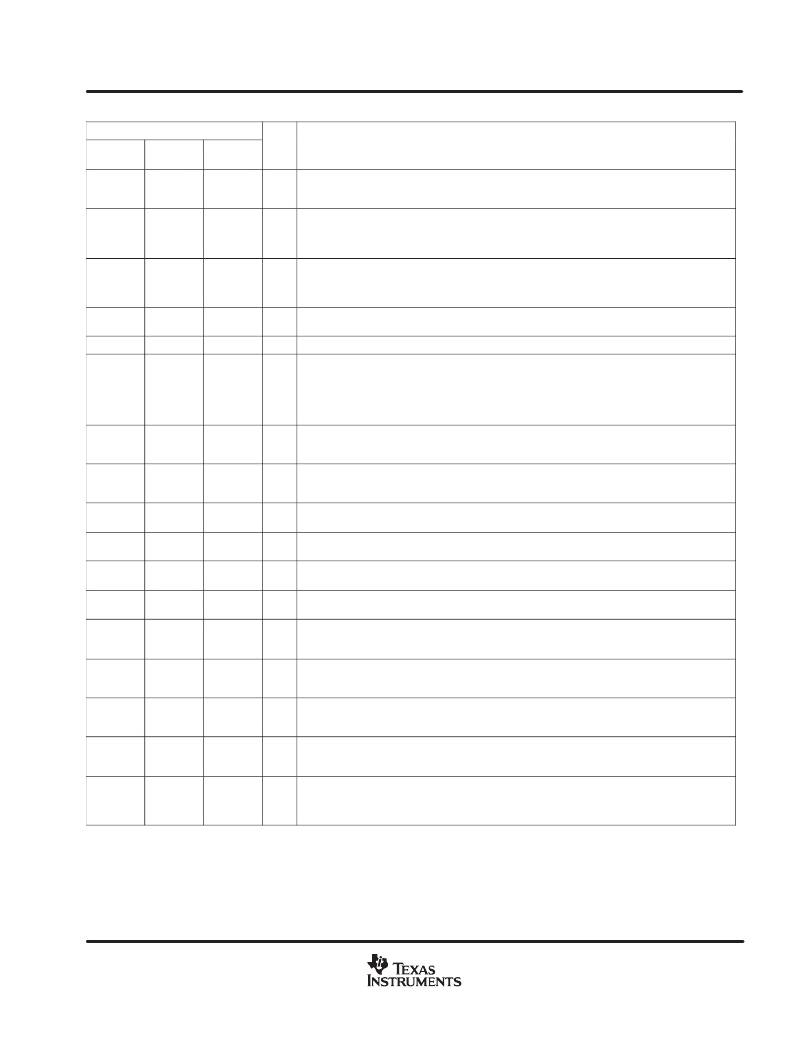
�TERMINAL� FUNCTIONS�
�TERMINAL�
�NAME�
�UCC2891�
�UCC2893�
�UCC2892�
�UCC2894�
�I/O�
�DESCRIPTION�
�This� output� drives� the� auxiliary� clamp� MOSFET� which� is� turned� on� when� the� main� PWM�
�AUX�
�12�
�12�
�O�
�switching� device� is� turned� off.� The� AUX� pin� can� directly� drive� the� auxiliary� switch� with� 2-A�
�source� turn-on� current� and� 2-A� sink� turn-off� current.�
�This� pin� is� used� to� sense� the� peak� current� utilized� for� current� mode� control� and� for� current�
�CS�
�7�
�7�
�I�
�limiting� functions.� The� peak� signal� which� can� be� applied� to� this� pin� before� pulse-by-pulse�
�current� limiting� activates� is� approximately� 0.75� V� for� the� UCC2891� and� UCC2893� and� 1.27� V�
�for� the� UCC2892� and� UCC2894.�
�This� pin� is� used� to� bring� the� error� signal� from� an� external� optocoupler� or� error� amplifier� into�
�FB�
�9�
�9�
�I�
�the� PWM� control� circuitry.� Often,� there� is� a� resistor� tied� from� FB� to� VREF,� and� an� optocoup-�
�ler� is� used� to� pull� the� control� pin� closer� to� GND� to� reduce� the� pulse� width� of� the� OUT� output�
�driving� the� main� power� switch� of� the� converter.�
�GND�
�LINEOV�
�6�
�?�
�6�
�16�
�?�
�I�
�This� pin� serves� as� the� fundamental� analog� ground� for� the� PWM� control� circuitry.� This� pin�
�should� be� connected� to� PGND� directly� at� the� device.�
�For� the� UCC2892/4,� provides� the� LINE� overvoltage� function.�
�This� pin� provides� a� means� to� accurately� enable/disable� the� power� converter� stage� by� moni-�
�toring� the� bulk� input� voltage� or� another� parameter.� When� the� circuit� initially� starts� (or� restarts�
�LINEUV�
�15�
�15�
�I�
�from� a� disabled� condition),� a� rising� input� on� LINEUV� enables� the� outputs� when� the� threshold�
�of� 1.27� V� is� crossed.� After� the� circuit� is� enabled,� then� a� falling� LINEUV� signal� disables� the�
�outputs� when� the� same� threshold� is� reached.� The� hysteresis� between� the� two� levels� is� pro-�
�grammed� using� an� internal� current� source.�
�This� output� pin� drives� the� main� PWM� switching� element� MOSFET� in� an� active� clamp� control-�
�OUT�
�13�
�13�
�O�
�ler.� It� can� directly� drive� an� N-channel� device� with� 2-A� source� turn-on� current� and� 2-A� sink�
�turn-off� current.� A� 10?k� ?� resistor� is� recommended� to� connect� this� pin� to� PGND.�
�The� PGND� should� serve� as� the� current� return� for� the� high-current� output� drivers� OUT� and�
�PGND�
�11�
�11�
�?�
�AUX.� Ideally,� the� current� path� from� the� outputs� to� the� switching� devices,� and� back� would� be�
�as� short� as� possible,� and� enclose� a� minimal� loop� area.�
�RSLOPE�
�RTDEL�
�RTOFF�
�RTON�
�SS/SD�
�8�
�1�
�3�
�2�
�10�
�8�
�1�
�3�
�2�
�10�
�I�
�I�
�I�
�I�
�I�
�A� resistor� connected� from� this� pin� to� GND� programs� an� internal� current� source� that� sets� the�
�slope� compensation� ramp� for� the� current� mode� control� circuitry.�
�A� resistor� from� this� pin� to� GND� programs� the� turn-on� delay� of� the� two� gate� drive� outputs� to�
�accommodate� the� resonant� transitions� of� the� active� clamp� power� converter.�
�A� resistor� connected� from� this� pin� to� GND� programs� an� internal� current� source� that� dis-�
�charges� the� internal� timing� capacitor.�
�A� resistor� connected� from� this� pin� to� GND� programs� an� internal� current� source� that� charges�
�the� internal� timing� capacitor.�
�A� capacitor� from� SS/SD� to� ground� is� charged� by� an� internal� current� source� of� IRTON� to� pro-�
�gram� the� soft-start� interval� for� the� controller.� During� a� fault� condition� this� capacitor� is� dis-�
�charged� by� a� current� source� equal� to� IRTON.�
�The� SYNC� pin� serves� as� a� unidirectional� synchronization� input� for� the� internal� oscillator.� The�
�SYNC�
�5�
�5�
�I�
�synchronization� function� is� implemented� such� that� the� user� programmable� maximum� duty�
�cycle� (set� by� RTON� and� RTOFF)� remains� accurate� during� synchronized� operation.�
�VDD�
�14�
�14�
�I�
�This� is� the� power� supply� for� the� device.� There� should� be� a� 1-� μ� F� capacitor� directly� from� VDD�
�to� PGND.� The� capacitor� value� should� be� minimum� 10� times� greater� than� that� on� VREF.�
�PGND� and� GND� should� be� connected� externally� and� directly� from� PGND� to� GND.�
�For� the� UCC2891� and� UCC2893,� this� pin� is� connected� to� the� input� power� rail� directly.� Inside�
�VIN�
�16�
�?�
�I�
�the� device,� a� high-voltage� start-up� device� is� utilized� to� provide� the� start-up� current� for� the�
�controller� until� a� bootstrap� type� bias� rail� becomes� available.�
�This� is� the� 5-V� reference� voltage� that� can� be� utilized� for� an� external� load� of� up� to� 5� mA.�
�VREF�
�4�
�4�
�O�
�Since� this� reference� provides� the� supply� rail� for� internal� logic,� it� should� be� bypassed� to�
�AGND� as� close� as� possible� to� the� device.� The� VREF� bias� profile� may� not� be� monotonic�
�before� VDD� reached� 5� V.�
�www.ti.com�
�7�
�相关PDF资料 |
PDF描述 |
|---|---|
| 3094-394KS | INDUCTOR RF CHIP 390UH 10% SMD |
| VI-J1K-EY-F4 | CONVERTER MOD DC/DC 40V 50W |
| UCC2894D | IC REG CTRLR FLYBK ISO CM 16SOIC |
| VI-J1K-EY-F3 | CONVERTER MOD DC/DC 40V 50W |
| 3094-334KS | INDUCTOR RF CHIP 330UH 10% SMD |
相关代理商/技术参数 |
参数描述 |
|---|---|
| UCC2891PWG4 | 功能描述:电流型 PWM 控制器 Current Mode Active Clamp RoHS:否 制造商:Texas Instruments 开关频率:27 KHz 上升时间: 下降时间: 工作电源电压:6 V to 15 V 工作电源电流:1.5 mA 输出端数量:1 最大工作温度:+ 105 C 安装风格:SMD/SMT 封装 / 箱体:TSSOP-14 |
| UCC2891PWR | 功能描述:电流型 PWM 控制器 Current Mode Active Clamp RoHS:否 制造商:Texas Instruments 开关频率:27 KHz 上升时间: 下降时间: 工作电源电压:6 V to 15 V 工作电源电流:1.5 mA 输出端数量:1 最大工作温度:+ 105 C 安装风格:SMD/SMT 封装 / 箱体:TSSOP-14 |
| UCC2891PWRG4 | 功能描述:电流型 PWM 控制器 Current Mode Active Clamp RoHS:否 制造商:Texas Instruments 开关频率:27 KHz 上升时间: 下降时间: 工作电源电压:6 V to 15 V 工作电源电流:1.5 mA 输出端数量:1 最大工作温度:+ 105 C 安装风格:SMD/SMT 封装 / 箱体:TSSOP-14 |
| UCC2892D | 功能描述:电流型 PWM 控制器 UCC289x Current Mode Active Clamp RoHS:否 制造商:Texas Instruments 开关频率:27 KHz 上升时间: 下降时间: 工作电源电压:6 V to 15 V 工作电源电流:1.5 mA 输出端数量:1 最大工作温度:+ 105 C 安装风格:SMD/SMT 封装 / 箱体:TSSOP-14 |
| UCC2892DG4 | 功能描述:电流型 PWM 控制器 UCC289x Current Mode Active Clamp RoHS:否 制造商:Texas Instruments 开关频率:27 KHz 上升时间: 下降时间: 工作电源电压:6 V to 15 V 工作电源电流:1.5 mA 输出端数量:1 最大工作温度:+ 105 C 安装风格:SMD/SMT 封装 / 箱体:TSSOP-14 |
发布紧急采购,3分钟左右您将得到回复。