- 您现在的位置:买卖IC网 > PDF目录11188 > UPD78F9512GR-JJG-A (Renesas Electronics America)MCU 8BIT SGL CHIP 16PIN PDF资料下载
参数资料
| 型号: | UPD78F9512GR-JJG-A |
| 厂商: | Renesas Electronics America |
| 文件页数: | 69/175页 |
| 文件大小: | 0K |
| 描述: | MCU 8BIT SGL CHIP 16PIN |
| 标准包装: | 400 |
| 系列: | 78K0S/Kx1+ |
| 核心处理器: | 78K0S |
| 芯体尺寸: | 8-位 |
| 速度: | 10MHz |
| 外围设备: | LVD,POR,PWM,WDT |
| 输入/输出数: | 13 |
| 程序存储器容量: | 4KB(4K x 8) |
| 程序存储器类型: | 闪存 |
| RAM 容量: | 128 x 8 |
| 电压 - 电源 (Vcc/Vdd): | 2 V ~ 5.5 V |
| 振荡器型: | 内部 |
| 工作温度: | -40°C ~ 85°C |
| 封装/外壳: | 16-SSOP(0.173",4.40mm 宽) |
| 包装: | 托盘 |
第1页第2页第3页第4页第5页第6页第7页第8页第9页第10页第11页第12页第13页第14页第15页第16页第17页第18页第19页第20页第21页第22页第23页第24页第25页第26页第27页第28页第29页第30页第31页第32页第33页第34页第35页第36页第37页第38页第39页第40页第41页第42页第43页第44页第45页第46页第47页第48页第49页第50页第51页第52页第53页第54页第55页第56页第57页第58页第59页第60页第61页第62页第63页第64页第65页第66页第67页第68页当前第69页第70页第71页第72页第73页第74页第75页第76页第77页第78页第79页第80页第81页第82页第83页第84页第85页第86页第87页第88页第89页第90页第91页第92页第93页第94页第95页第96页第97页第98页第99页第100页第101页第102页第103页第104页第105页第106页第107页第108页第109页第110页第111页第112页第113页第114页第115页第116页第117页第118页第119页第120页第121页第122页第123页第124页第125页第126页第127页第128页第129页第130页第131页第132页第133页第134页第135页第136页第137页第138页第139页第140页第141页第142页第143页第144页第145页第146页第147页第148页第149页第150页第151页第152页第153页第154页第155页第156页第157页第158页第159页第160页第161页第162页第163页第164页第165页第166页第167页第168页第169页第170页第171页第172页第173页第174页第175页
CHAPTER 9 A/D CONVERTER (
μPD78F921x ONLY)
User’s Manual U16994EJ6V0UD
158
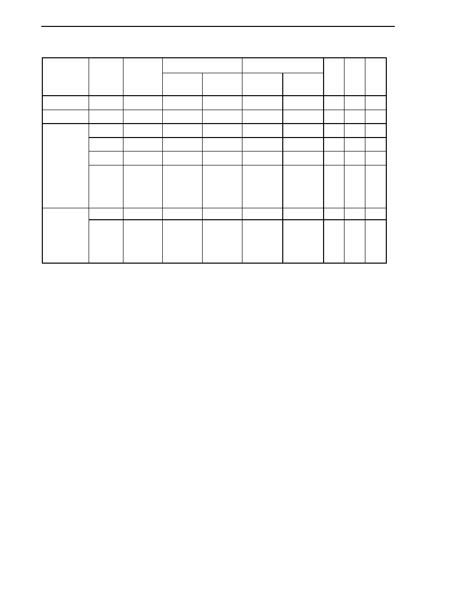
Table 9-1. Sampling Time and A/D Conversion Time
fXP = 8 MHz
fXP = 10 MHz
Reference
Voltage
Range
Note 1
Sampling
Time
Note 2
Conversion
Time
Note 3
Sampling
Time
Note 2
Conversion
Time
Note 3
Sampling
Time
Note 2
Conversion
Time
Note 3
FR2
FR1
FR0
VDD
≥ 4.5 V
12/fXP
36/fXP
1.5
μs
4.5
μs
1.2
μs
3.6
μs
0
VDD
≥ 4.0 V
24/fXP
72/fXP
3.0
μs
9.0
μs
2.4
μs
7.2
μs
1
0
96/fXP
144/fXP
12.0
μs
18.0
μs
9.6
μs
14.4
μs
1
0
48/fXP
96/fXP
6.0
μs
12.0
μs
4.8
μs
9.6
μs
1
0
1
48/fXP
72/fXP
6.0
μs
9.0
μs
4.8
μs
7.2
μs
0
1
0
VDD
≥ 2.85 V
24/fXP
48/fXP
3.0
μs
6.0
μs
Setting
prohibited
Note 4
(2.4
μs)
Setting
prohibited
Note 4
(4.8
μs)
0
1
176/fXP
224/fXP
22.0
μs
28.0
μs
17.6
μs
22.4
μs
1
VDD
≥ 2.7 V
88/fXP
112/fXP
11.0
μs
14.0
μs
Setting
prohibited
Note 4
(8.8
μs)
Setting
prohibited
Note 4
(11.2
μs)
0
1
Notes 1.
Be sure to set the FR2, FR1, and FR0, in accordance with the reference voltage so that Notes 2 and 3
below are satisfied.
Example When VDD
≥ 2.7 V, fXP = 8 MHz
The sampling time is 11.0
μs or more and the A/D conversion time is 14.0 μs or more and 100 μs or
less.
Set FR2, FR1, and FR0 = 0, 1, 1 or 1, 1, 1.
2.
Set the sampling time as follows.
VDD ≥ 4.5 V:
1.0
μs or more
VDD ≥ 4.0 V:
2.4
μs or more
VDD ≥ 2.85 V:
3.0
μs or more
VDD ≥ 2.7 V:
11.0
μs or more
3.
Set the A/D conversion time as follows.
VDD ≥ 4.5 V:
3.0
μs or more and less than 100 μs
VDD ≥ 4.0 V:
4.8
μs or more and less than 100 μs
VDD ≥ 2.85 V:
6.0
μs or more and less than 100 μs
VDD ≥ 2.7 V:
14.0
μs or more and less than 100 μs
4.
Setting is prohibited because the values do not satisfy the condition of Notes 2 or 3.
Caution
The above sampling time and conversion time do not include the clock frequency error. Select
the sampling time and conversion time such that Notes 2 and 3 above are satisfied, while taking
the clock frequency error into consideration (an error margin maximum of
±5% when using the
high-speed internal oscillator).
Remarks 1.
fXP: Oscillation frequency of clock to peripheral hardware
2.
The conversion time refers to the total of the sampling time and the time from successively
comparing with the sampling value until the conversion result is output.
相关PDF资料 |
PDF描述 |
|---|---|
| VI-J3D-IW-F3 | CONVERTER MOD DC/DC 85V 100W |
| C8051F826-GS | IC MCU 8BIT 8KB FLASH 16SOIC |
| VI-J3D-IW-F2 | CONVERTER MOD DC/DC 85V 100W |
| VI-J3B-IW-F4 | CONVERTER MOD DC/DC 95V 100W |
| VI-J3B-IW-F3 | CONVERTER MOD DC/DC 95V 100W |
相关代理商/技术参数 |
参数描述 |
|---|---|
| UPD78F9801GB-8ES-A | 制造商:Renesas Electronics Corporation 功能描述: |
| UPD78F9842GB-8ES | 制造商:Renesas Electronics Corporation 功能描述: |
| UPD78F9842GB-8ES-A | 制造商:Renesas Electronics Corporation 功能描述: |
| UPD78F9850AMC(A)-5A4-A | 制造商:Renesas Electronics Corporation 功能描述: |
| UPD78F9852GB(A)-8ES | 制造商:Renesas Electronics Corporation 功能描述: |
发布紧急采购,3分钟左右您将得到回复。