- 您现在的位置:买卖IC网 > PDF目录300087 > VCA2614Y/2K (TEXAS INSTRUMENTS INC) SPECIALTY ANALOG CIRCUIT, PQFP32 PDF资料下载
参数资料
| 型号: | VCA2614Y/2K |
| 厂商: | TEXAS INSTRUMENTS INC |
| 元件分类: | 模拟信号调理 |
| 英文描述: | SPECIALTY ANALOG CIRCUIT, PQFP32 |
| 封装: | PLASTIC, TQFP-32 |
| 文件页数: | 11/18页 |
| 文件大小: | 519K |
| 代理商: | VCA2614Y/2K |
VCA2614
2
SBOS185D
www.ti.com
ELECTRICAL CHARACTERISTICS
At TA = +25°C, VDD = 5V, load resistance = 500 on each output to ground differential output (2Vp-p), MGS = 011, and fIN = 5MHz, unless otherwise noted.
ELECTROSTATIC
DISCHARGE SENSITIVITY
This integrated circuit can be damaged by ESD. Texas Instru-
ments recommends that all integrated circuits be handled with
appropriate precautions. Failure to observe proper handling
and installation procedures can cause damage.
ESD damage can range from subtle performance degrada-
tion to complete device failure. Precision integrated circuits
may be more susceptible to damage because very small
parametric changes could cause the device not to meet its
published specifications.
ABSOLUTE MAXIMUM RATINGS(1)
Power Supply (+VS) ............................................................................. +6V
Analog Input ............................................................. –0.3V to (+VS + 0.3V)
Logic Input ............................................................... –0.3V to (+VS + 0.3V)
Case Temperature ......................................................................... +100
°C
Junction Temperature .................................................................... +150
°C
Storage Temperature ...................................................... –40
°C to +150°C
NOTE: (1) Stresses above those listed under “Absolute Maximum Ratings”
may cause permanent damage to the device. Exposure to absolute maximum
conditions for extended periods may affect device reliability.
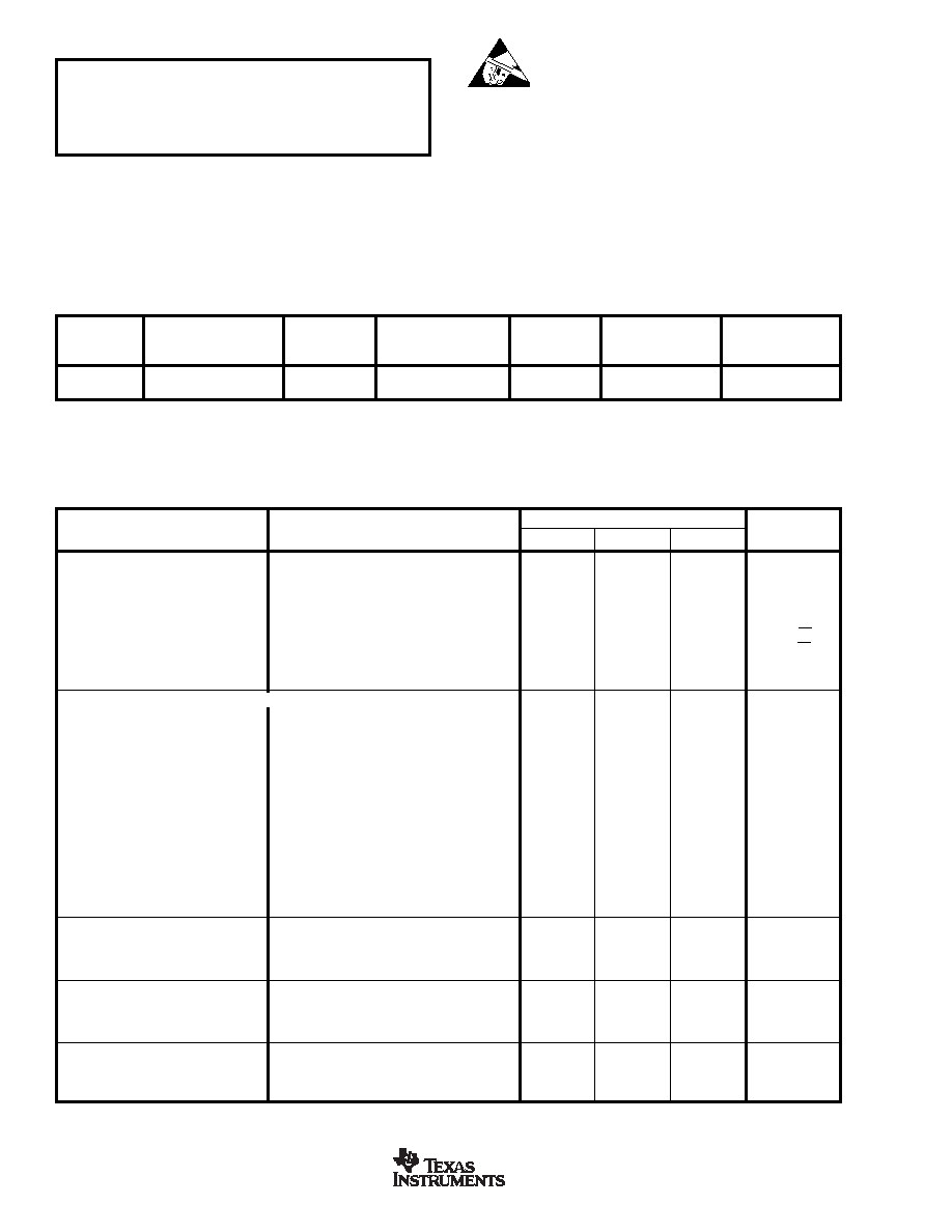
SPECIFIED
PACKAGE
TEMPERATURE
PACKAGE
ORDERING
TRANSPORT
PRODUCT
PACKAGE-LEAD
DESIGNATOR(1)
RANGE
MARKING
NUMBER
MEDIA, QUANTITY
VCA2614Y
TQFP-32 Surface-Mount
PBS
–40
°C to +85°C
VCA2614Y
VCA2614Y/250
Tape and Reel, 250
""
"""
VCA2614Y/2K
Tape and Reel, 2000
NOTE: (1) For the most current specifications and package information, refer to our web site at www.ti.com.
PACKAGE/ORDERING INFORMATION
VCA2614Y
PARAMETER
CONDITIONS
MIN
TYP
MAX
UNITS
BUFFER
Input Resistance
600
k
Input Capacitance
5pF
Input Bias Current
1nA
Maximum Input Voltage
1
Vp-p
Input Voltage Noise
MGS = 111, PGA Gain = 44.2dB, RS = 50
4.8
nV/√Hz
Input Current Noise
Independent of Gain
350
fA/√Hz
Noise Figure
RF = 550, PGA Gain = 44.2dB, RS = 75
13
dB
Bandwidth
100
MHz
PROGRAMMABLE VARIABLE GAIN AMPLIFIER
Peak Input Voltage
1
Vp-p
–3dB Bandwidth
40
MHz
Slew Rate
300
V/
s
Output Signal Range
RL ≥ 500 Each Side to Ground
2.5
±1V
Output Impedance
f = 5MHz
1
Output Short-Circuit Current
±40
mA
3rd-Harmonic Distortion
f = 5MHz, VOUT = 2Vp-p, VCACNTL = 3.0V
–45
–60
dBc
2nd-Harmonic Distortion
f = 5MHz, VOUT = 2Vp-p, VCACNTL = 3.0V
–45
–50
dBc
Overload Performance (2nd-Harmonic
Input Signal = 1Vp-p, MGS = 111, VCACNTL = 2V
–40 to –45
dB
Distortion)
Time Delay
5ns
IMD, 2-Tone
VOUT = 2Vp-p, f = 9.95MHz
–59
dBc
Crosstalk
70
dB
Group Delay Variation
1MHz < f < 10MHz, Full Gain Range
13
ns
ACCURACY
Gain Slope
10.5
dB/V
Gain Error
±2(1)
dB
Output Offset Voltage
±50
mV
GAIN CONTROL INTERFACE
Input Voltage (VCACNTL) Range
0.2 to 3.0
V
Input Resistance
1M
Response Time
40dB Gain Change, MGS = 111
0.2
s
POWER SUPPLY
Specified Operating Range
4.75
5.0
5.25
V
Power Dissipation
Operating, Each Channel
120
150
mW
Power-Down
9.2
mW
NOTE: (1) Referenced to best fit dB-linear curve.
相关PDF资料 |
PDF描述 |
|---|---|
| VCA2615PFBR | SPECIALTY ANALOG CIRCUIT, PQFP48 |
| VCA2615RGZR | SPECIALTY ANALOG CIRCUIT, PQCC48 |
| VCA3-103-60M00 | CRYSTAL OSCILLATOR, CLOCK, 60 MHz, HCMOS/TTL OUTPUT |
| VCA3-A3F-FREQ | CRYSTAL OSCILLATOR, CLOCK, 0.32768 MHz - 160 MHz, CMOS OUTPUT |
| VCA3-A5D-FREQ | CRYSTAL OSCILLATOR, CLOCK, 0.32768 MHz - 160 MHz, CMOS OUTPUT |
相关代理商/技术参数 |
参数描述 |
|---|---|
| VCA2615 | 制造商:BB 制造商全称:BB 功能描述:Dual, Variable Gain Amplifier |
| VCA2615EVM | 功能描述:放大器 IC 开发工具 VCA2615 Eval Mod RoHS:否 制造商:International Rectifier 产品:Demonstration Boards 类型:Power Amplifiers 工具用于评估:IR4302 工作电源电压:13 V to 23 V |
| VCA2615PFBR | 功能描述:特殊用途放大器 2Ch Variable Gain Amplifier RoHS:否 制造商:Texas Instruments 通道数量:Single 共模抑制比(最小值): 输入补偿电压: 工作电源电压:3 V to 5.5 V 电源电流:5 mA 最大功率耗散: 最大工作温度:+ 70 C 最小工作温度:- 40 C 安装风格:SMD/SMT 封装 / 箱体:QFN-20 封装:Reel |
| VCA2615PFBT | 功能描述:特殊用途放大器 2Ch Variable Gain Amplifier RoHS:否 制造商:Texas Instruments 通道数量:Single 共模抑制比(最小值): 输入补偿电压: 工作电源电压:3 V to 5.5 V 电源电流:5 mA 最大功率耗散: 最大工作温度:+ 70 C 最小工作温度:- 40 C 安装风格:SMD/SMT 封装 / 箱体:QFN-20 封装:Reel |
| VCA2615RGZR | 功能描述:特殊用途放大器 2-Channel Variable Gain Amplifier RoHS:否 制造商:Texas Instruments 通道数量:Single 共模抑制比(最小值): 输入补偿电压: 工作电源电压:3 V to 5.5 V 电源电流:5 mA 最大功率耗散: 最大工作温度:+ 70 C 最小工作温度:- 40 C 安装风格:SMD/SMT 封装 / 箱体:QFN-20 封装:Reel |
发布紧急采购,3分钟左右您将得到回复。