- 您现在的位置:买卖IC网 > PDF目录300087 > VCA2614Y/2K (TEXAS INSTRUMENTS INC) SPECIALTY ANALOG CIRCUIT, PQFP32 PDF资料下载
参数资料
| 型号: | VCA2614Y/2K |
| 厂商: | TEXAS INSTRUMENTS INC |
| 元件分类: | 模拟信号调理 |
| 英文描述: | SPECIALTY ANALOG CIRCUIT, PQFP32 |
| 封装: | PLASTIC, TQFP-32 |
| 文件页数: | 3/18页 |
| 文件大小: | 519K |
| 代理商: | VCA2614Y/2K |
11
SBOS185D
www.ti.com
VCA2614
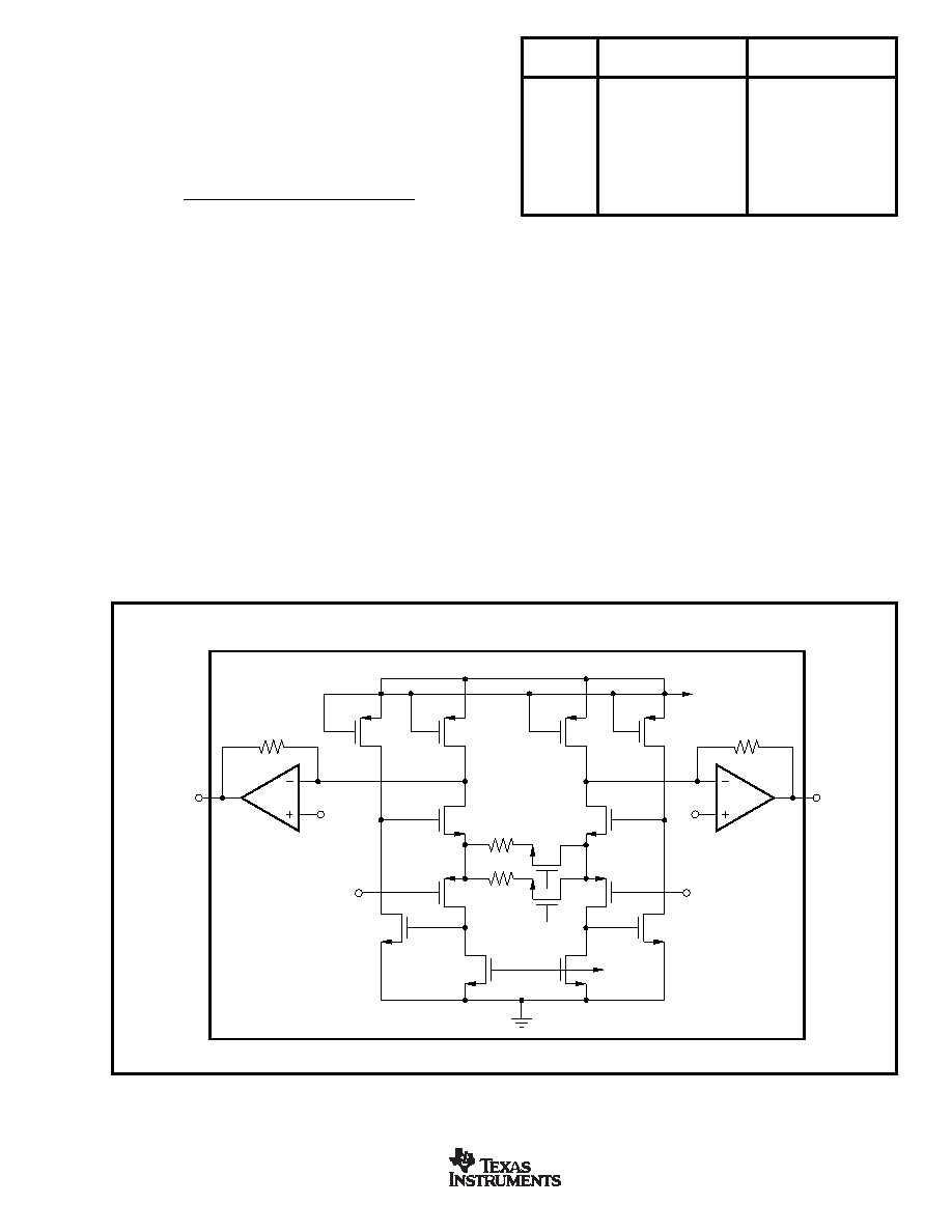
PGA POST-AMPLIFIER
Figure 5 shows a simplified circuit diagram of the PGA block.
As stated before, the input to the PGA is AC-coupled by an
internal capacitor. Provisions are made so that an external
capacitor can be placed in parallel with the internal capacitor,
thus lowering the usable low-frequency bandwidth. The low-
frequency bandwidth is set by the following equation:
1
2
500
220
+
(
)
(
)
π
kpF
CEXTERNAL
where CEXTERNAL is the external capacitor value in picofarads.
Care should be taken to avoid using too large a value of
capacitor, as this can increase the power-on delay time.
As described previously, the PGA gain is programmed with
the same MGS bits that control the VCA maximum attenua-
tion factor. Specifically, the maximum PGA gain at each
MGS setting is the inverse (reciprocal) of the maximum VCA
attenuation at that setting. Therefore, the VCA + PGA overall
gain will always be 0dB (unity) when the analog VCACNTL
input is set to 0V (the maximum attenuation for VCA). For
VCACNTL = 3V (no attenuation), the VCA + PGA gain will be
controlled by the programmed PGA gain. For clarity, the gain
and attenuation factors are detailed in Table I.
The PGA architecture converts the single-ended signal from
the VCA into a differential signal. Low input noise was also
a requirement of the PGA design due to the large amount of
signal attenuation that can be asserted before the PGA. At
minimum VCA attenuation (used for small input signals), the
MGS
ATTENUATOR GAIN
ATTENUATOR +
SETTING
VCACNTL = 0.02V to 3V
DIFFERENTIAL PGA GAIN
000
Not Valid
001
–24.1dB to 0dB
2.6dB to 26.7dB
010
–26.9dB to 0dB
2.6dB to 29.5dB
011
–29.5dB to 0dB
3.0dB to 35.6dB
100
–32.4dB to 0dB
3.1dB to 35.5dB
101
–34.8dB to 0dB
3.4dB to 38.3dB
110
–37.3dB to 0dB
3.7dB to 44.1dB
111
–40.0dB to 0dB
4.1dB to 44.2dB
R
S1
R
L
R
S2
VCA
OUTP
+In
Q
11
Q
3
Q
4
Q
5
Q
1
V
CM
Q
2
VCA
OUTN
Q
9
Q
8
Q
13
Q
14
Q
7
Q
6
Q
12
V
DD
V
CM
R
L
Q
10
–In
To Bias
Circuitry
To Bias
Circuitry
FIGURE 5. Simplified Block Diagram of the PGA Section with the VCA2614.
TABLE I. MGS Settings.
input buffer noise dominates; at maximum VCA attenuation
(large input signals), the PGA noise dominates. Note that if
the PGA output is used single-ended, the apparent gain will
be 6dB lower.
LAYOUT CONSIDERATIONS
The VCA2614 is an analog amplifier capable of high gain.
When working on a PCB layout for the VCA2614, it is
recommended to utilize a solid ground plane that is con-
nected to analog ground. This helps to maximize the noise
performance of the VCA2614.
Adequate power-supply decoupling must be used in order to
achieve the best possible performance. Decoupling capaci-
tors on the VCACNTL voltage should also be used to help
minimize noise. Recommended values can be obtained from
the layout diagram of Figure 6.
相关PDF资料 |
PDF描述 |
|---|---|
| VCA2615PFBR | SPECIALTY ANALOG CIRCUIT, PQFP48 |
| VCA2615RGZR | SPECIALTY ANALOG CIRCUIT, PQCC48 |
| VCA3-103-60M00 | CRYSTAL OSCILLATOR, CLOCK, 60 MHz, HCMOS/TTL OUTPUT |
| VCA3-A3F-FREQ | CRYSTAL OSCILLATOR, CLOCK, 0.32768 MHz - 160 MHz, CMOS OUTPUT |
| VCA3-A5D-FREQ | CRYSTAL OSCILLATOR, CLOCK, 0.32768 MHz - 160 MHz, CMOS OUTPUT |
相关代理商/技术参数 |
参数描述 |
|---|---|
| VCA2615 | 制造商:BB 制造商全称:BB 功能描述:Dual, Variable Gain Amplifier |
| VCA2615EVM | 功能描述:放大器 IC 开发工具 VCA2615 Eval Mod RoHS:否 制造商:International Rectifier 产品:Demonstration Boards 类型:Power Amplifiers 工具用于评估:IR4302 工作电源电压:13 V to 23 V |
| VCA2615PFBR | 功能描述:特殊用途放大器 2Ch Variable Gain Amplifier RoHS:否 制造商:Texas Instruments 通道数量:Single 共模抑制比(最小值): 输入补偿电压: 工作电源电压:3 V to 5.5 V 电源电流:5 mA 最大功率耗散: 最大工作温度:+ 70 C 最小工作温度:- 40 C 安装风格:SMD/SMT 封装 / 箱体:QFN-20 封装:Reel |
| VCA2615PFBT | 功能描述:特殊用途放大器 2Ch Variable Gain Amplifier RoHS:否 制造商:Texas Instruments 通道数量:Single 共模抑制比(最小值): 输入补偿电压: 工作电源电压:3 V to 5.5 V 电源电流:5 mA 最大功率耗散: 最大工作温度:+ 70 C 最小工作温度:- 40 C 安装风格:SMD/SMT 封装 / 箱体:QFN-20 封装:Reel |
| VCA2615RGZR | 功能描述:特殊用途放大器 2-Channel Variable Gain Amplifier RoHS:否 制造商:Texas Instruments 通道数量:Single 共模抑制比(最小值): 输入补偿电压: 工作电源电压:3 V to 5.5 V 电源电流:5 mA 最大功率耗散: 最大工作温度:+ 70 C 最小工作温度:- 40 C 安装风格:SMD/SMT 封装 / 箱体:QFN-20 封装:Reel |
发布紧急采购,3分钟左右您将得到回复。