- 您现在的位置:买卖IC网 > PDF目录17002 > VNCLO-PSU-EU (FTDI, Future Technology Devices International Ltd)POWER SUPPLY FOR VNCLO-MB1A EU PDF资料下载
参数资料
| 型号: | VNCLO-PSU-EU |
| 厂商: | FTDI, Future Technology Devices International Ltd |
| 文件页数: | 15/25页 |
| 文件大小: | 0K |
| 描述: | POWER SUPPLY FOR VNCLO-MB1A EU |
| 应用说明: | Vinco LCD Interface Example Vinco Graphics Display Example Vinco Volt Meter Example Using the Vinco Libraries |
| 产品变化通告: | Name Change to Vinco 22/Apr/2011 |
| 特色产品: | Vinco Development Board |
| 标准包装: | 1 |
| 系列: | Vinco |
| 附件类型: | 电源 |
| 适用于相关产品: | FTDI Vinco 卡 |
| 其它名称: | 768-1093 |
�� �
�
�Document� Reference� No.:� FT_000327�
�Vinco� Development� Module� Datasheet� Version� 2.01�
�Clearance� No.:� FTDI#173�
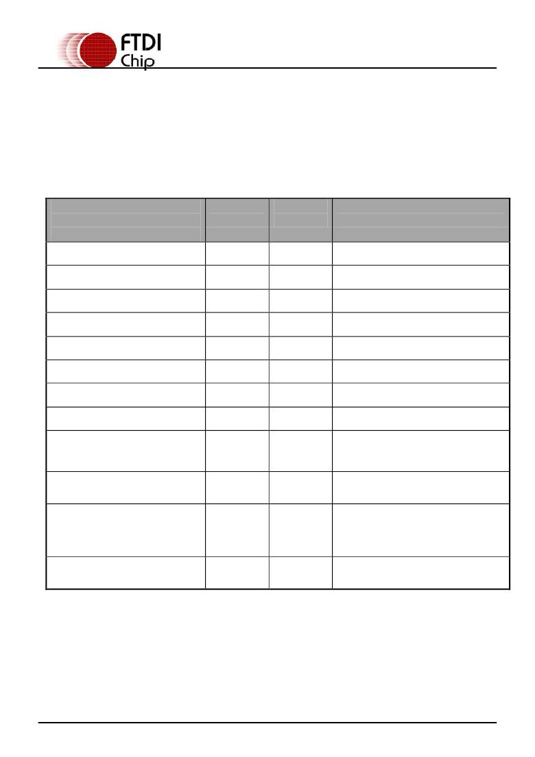
�4.3� Parallel� FIFO� Interface� -� Asynchronous� Mode�
�The� Parallel� FIFO� Asynchronous� mode� is� functionally� the� same� as� the� Parallel� FIFO� Interface� available� in�
�the� FTDI� VDIP1� module� and� has� an� eight� bit� data� bus,� individual� read� and� write� strobes� and� two�
�hardware� flow� control� signals.�
�4.3.1� Signal� Description� -� Parallel� FIFO� Interface�
�The� Parallel� FIFO� Interface� signals� can� be� programmed� to� a� choice� of� available� I/O� pins.� Table� 4.4� shows�
�the� Parallel� FIFO� Interface� signals� and� the� pins� that� they� can� be� mapped.� Details� of� the� operation� and�
�timing� can� be� found� in� the� VNC2� datasheet.�
�Available� Pins�
�J2-1,� J2-5,� J3-2,� J3-5,� J4-6,� J5-7,� J6-1,�
�J6-5�
�J2-2,� J2-6,� J3-1,� J3-6,� J4-4,� J5-1,� J5-4,�
�J5-8,� J6-2,� J6-6�
�J1-1,� J2-3,� J3-3,� J3-7,� J4-1,� J4-5,� J5-2,�
�J5-5,� J6-3,� J6-7�
�J1-2,� J2-4,� J3-4,� J3-8,� J4-2,� J4-3,� J5-3,�
�J5-6,� J6-4,� J6-8�
�J2-1,� J2-5,� J3-2,� J3-5,� J4-6,� J5-7,� J6-1,�
�J6-5�
�J2-2,� J2-6,� J3-1,� J3-6,� J4-4,� J5-1,� J5-4,�
�J5-8,� J6-2,� J6-6�
�J1-1,� J2-3,� J3-3,� J3-7,� J4-1,� J4-5,� J5-2,�
�J5-5,� J6-3,� J6-7�
�J1-2,� J2-4,� J3-4,� J3-8,� J4-2,� J4-3,� J5-3,�
�J5-6,� J6-4,� J6-8�
�J2-1,� J2-5,� J3-2,� J3-5,� J4-6,� J5-7,� J6-1,�
�J6-5�
�J2-2,� J2-6,� J3-1,� J3-6,� J4-4,� J5-1,� J5-4,�
�J5-8,� J6-2,� J6-6�
�J1-1,� J2-3,� J3-3,� J3-7,� J4-1,� J4-5,� J5-2,�
�J5-5,� J6-3,� J6-7�
�J1-2,� J2-4,� J3-4,� J3-8,� J4-2,� J4-3,� J5-3,�
�J5-6,� J6-4,� J6-8�
�Name�
�fifo_data[0]�
�fifo_data[1]�
�fifo_data[2]�
�fifo_data[3]�
�fifo_data[4]�
�fifo_data[5]�
�fifo_data[6]�
�fifo_data[7]�
�fifo_rxf#�
�fifo_txe#�
�fifo_rd#�
�fifo_wr#�
�Type�
�I/O�
�I/O�
�I/O�
�I/O�
�I/O�
�I/O�
�I/O�
�I/O�
�Output�
�Output�
�Input�
�Input�
�Description�
�FIFO� data� bus� Bit� 0�
�FIFO� data� bus� Bit� 1�
�FIFO� data� bus� Bit� 2�
�FIFO� data� bus� Bit� 3�
�FIFO� data� bus� Bit� 4�
�FIFO� data� bus� Bit� 5�
�FIFO� data� bus� Bit� 6�
�FIFO� data� bus� Bit� 7�
�When� high,� do� not� read� data� from� the� FIFO.�
�When� low,� there� is� data� available� in� the� FIFO�
�which� can� be� read� by� strobing� RD#� low,� then�
�high.�
�When� high,� do� not� write� data� into� the� FIFO.�
�When� low,� data� can� be� written� into� the� FIFO�
�by� strobing� WR� high,� then� low.�
�Enables� the� current� FIFO� data� byte� on�
�D0...D7� when� low.� Fetches� the� next� FIFO�
�data� byte� (if� available)� from� the� receive� FIFO�
�buffer� when� RD#� goes� from� high� to� low�
�Writes� the� data� byte� on� the� D0...D7� pins� into�
�the� transmit� FIFO� buffer� when� WR� goes� from�
�high� to� low.�
�Table� 4.4� –� Data� and� Control� Bus� Signal� Mode� Options� –� Parallel� FIFO� Interface�
�Note:�
�1.� #� defines� active� low� signals.�
�2.� Also� PWM� outputs� can� be� routed� to� any� of� the� pins� listed� in� table� 4.1�
�Copyright� ?� 2012� Future� Technology� Devices� International� Limited�
�11�
�相关PDF资料 |
PDF描述 |
|---|---|
| HPL1005-4N3 | INDUCTOR 4.3NH +/-0.2NH 0402 |
| 0982660835 | CBL 15POS 0.5MM JMPR TYPE A 2" |
| EBM12DSAI | CONN EDGECARD 24POS R/A .156 SLD |
| 0982660834 | CBL 15POS 0.5MM JMPR TYPE D 2" |
| EEM28DRST | CONN EDGECARD 56POS DIP .156 SLD |
相关代理商/技术参数 |
参数描述 |
|---|---|
| VNCLO-PSU-UK | 功能描述:插入式交流适配器 Vinco+9V/1A UK Power Supply Unit RoHS:否 制造商:Phihong 地区:Universal 安装风格:Wall, Interchangeable Plug 输入电压范围:90 VAC to 264 VAC 输出端数量:1 输出功率额定值:5 W 输出电压(通道 1):5 V 输出电流(通道 1):1 A 直流输出连接器:USB Type A 随附/必需的交流插头:Required 商用/医用:Commercial 效率:Level V |
| VNCLO-PSU-US | 制造商:FTDI 制造商全称:FTDI 功能描述:Vinculo Development Module |
| VNCLO-PSU-USA | 功能描述:插入式交流适配器 Vinco +9V/1A USA Pwr Supply Unit RoHS:否 制造商:Phihong 地区:Universal 安装风格:Wall, Interchangeable Plug 输入电压范围:90 VAC to 264 VAC 输出端数量:1 输出功率额定值:5 W 输出电压(通道 1):5 V 输出电流(通道 1):1 A 直流输出连接器:USB Type A 随附/必需的交流插头:Required 商用/医用:Commercial 效率:Level V |
| VNCLO-SHLD1A | 制造商:FTDI 制造商全称:FTDI 功能描述:Vinculo Development Module |
| VNCLO-SHLD-1A | 功能描述:模块配件 Vinco Prototyping Shield Accessory RoHS:否 制造商:Lantronix 产品: 用于: |
发布紧急采购,3分钟左右您将得到回复。