- 您现在的位置:买卖IC网 > PDF目录361766 > W181-01X MISCELLANEOUS CLOCK GENERATOR|CMOS|TSSOP|14PIN|PLASTIC PDF资料下载
参数资料
| 型号: | W181-01X |
| 英文描述: | MISCELLANEOUS CLOCK GENERATOR|CMOS|TSSOP|14PIN|PLASTIC |
| 中文描述: | 杂项时钟发生器|的CMOS | TSSOP封装| 14PIN |塑料 |
| 文件页数: | 3/9页 |
| 文件大小: | 160K |
| 代理商: | W181-01X |
W181
3
Overview
The W181 products are one series of devices in the Cypress
PREMIS family. The PREMIS family incorporates the latest
advances in PLL spread spectrum frequency synthesizer tech-
niques. By frequency modulating the output with a low-
frequency carrier, peak EMI is greatly reduced. Use of this
technology allows systems to pass increasingly difficult EMI
testing without resorting to costly shielding or redesign.
In a system, not only is EMI reduced in the various clock lines,
but also in all signals which are synchronized to the clock.
Therefore, the benefits of using this technology increase with
the number of address and data lines in the system. The Sim-
plified Block Diagram on page 1 shows a simple implementa-
tion.
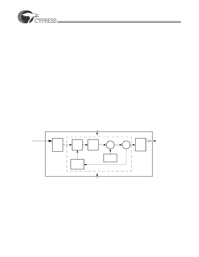
Functional Description
The W181 uses a phase-locked loop (PLL) to frequency mod-
ulate an input clock. The result is an output clock whose fre-
quency is slowly swept over a narrow band near the input sig-
nal. The basic circuit topology is shown in
Figure 1
. The input
reference signal is divided by Q and fed to the phase detector.
A signal from the VCO is divided by P and fed back to the
phase detector also. The PLL will force the frequency of the
VCO output signal to change until the divided output signal
and the divided reference signal match at the phase detector
input. The output frequency is then equal to the ratio of P/Q
times the reference frequency. (Note: For the W181 the output
frequency is equal to the input frequency.) The unique feature
of the Spread Spectrum Frequency Timing Generator is that a
modulating waveform is superimposed at the input to the VCO.
This causes the VCO output to be slowly swept across a pre-
determined frequency band.
Because the modulating frequency is typically 1000 times
slower than the fundamental clock, the spread spectrum pro-
cess has little impact on system performance.
Frequency Selection With SSFTG
In Spread Spectrum Frequency Timing Generation, EMI re-
duction depends on the shape, modulation percentage, and
frequency of the modulating waveform. While the shape and
frequency of the modulating waveform are fixed for a given
frequency, the modulation percentage may be varied.
Using frequency select bits (FS1:2 pins), the frequency range
can be set. Spreading percentage is set to be
–
1.25% (see
Table 1
).
A larger spreading percentage improves EMI reduction. How-
ever, large spread percentages may either exceed system
maximum frequency ratings or lower the average frequency to
a point where performance is affected. For these reasons,
spreading percentages between 0.5% and 2.5% are most
common.
Freq.
Divider
Q
Phase
Detector
Modulating
Waveform
VCO
Post
Dividers
CLKOUT
(EMI suppressed)
Charge
Pump
Feedback
DiP
PLL
GND
V
DD
Σ
Clock Input
Reference Input
Figure 1. Functional Block Diagram
相关PDF资料 |
PDF描述 |
|---|---|
| W181-02G | MISCELLANEOUS CLOCK GENERATOR|CMOS|SOP|8PIN|PLASTIC |
| W181-03G | Miscellaneous Clock Generator |
| W182G | MISCELLANEOUS CLOCK GENERATOR|CMOS|SOP|14PIN|PLASTIC |
| W183G | MISCELLANEOUS CLOCK GENERATOR|CMOS|SOP|14PIN|PLASTIC |
| W184H | MISCELLANEOUS CLOCK GENERATOR|CMOS|SSOP|24PIN|PLASTIC |
相关代理商/技术参数 |
参数描述 |
|---|---|
| W181-02G | 制造商:Cypress Semiconductor 功能描述:PLL Frequency Synthesizer Single 8-Pin SOIC |
| W181-02GI | 制造商:Cypress Semiconductor 功能描述:PLL Frequency Synthesizer Single 8-Pin SOIC |
| W181-02GT | 制造商:Cypress Semiconductor 功能描述:PLL Frequency Synthesizer Single 8-Pin SOIC T/R |
| W181-02SZT | 制造商:Rochester Electronics LLC 功能描述:- Tape and Reel |
| W18103G | 制造商:Cypress Semiconductor 功能描述: |
发布紧急采购,3分钟左右您将得到回复。