- 您现在的位置:买卖IC网 > PDF目录361766 > W181-03G Miscellaneous Clock Generator PDF资料下载
参数资料
| 型号: | W181-03G |
| 英文描述: | Miscellaneous Clock Generator |
| 中文描述: | 杂项时钟发生器 |
| 文件页数: | 1/9页 |
| 文件大小: | 160K |
| 代理商: | W181-03G |
Peak Reducing EMI Solution
W181
Cypress Semiconductor Corporation
3901 North First Street
San Jose
CA 95134
408-943-2600
January 5, 2000, rev. *A
Features
Cypress PREMIS
family offering
Generates an EMI optimized clocking signal at the
output
Selectable input to output frequency
Single –1.25% or –3.75% down spread output
Integrated loop filter components
Operates with a 3.3V or 5V supply
Low power CMOS design
Available in 8-pin SOIC (Small Outline Integrated
Circuit) or 14-pin TSSOP (Thin Shrink Small Outline
Package)
Key Specifications
Supply Voltages: ...........................................V
DD
= 3.3V±5%
or V
DD
= 5V±10%
Frequency Range: ............................ 28 MHz
≤
F
in
≤
75 MHz
Crystal Reference Range.................. 28 MHz
≤
F
in
≤
40 MHz
Cycle to Cycle Jitter: ........................................300 ps (max)
Selectable Spread Percentage: ................–1.25% or –3.75%
Output Duty Cycle: ............................... 40/60% (worst case)
Output Rise and Fall Time: ...................................5 ns (max)
Table 1. Modulation Width Selection
SS%
Output
0
F
in
≥
F
out
≥
F
in
– 1.25%
F
in
≥
F
out
≥
F
in
– 3.75%
1
Table 2. Frequency Range Selection
W181 Option#
FS2
FS1
-01
(MHz)
-02
(MHz)
-03
(MHz)
0
0
28
≤
F
IN
≤
38
38
≤
F
IN
≤
48
46
≤
F
IN
≤
60
58
≤
F
IN
≤
75
28
≤
F
IN
≤
38
38
≤
F
IN
≤
48
N/A
N/A
0
1
N/A
1
0
46
≤
F
IN
≤
60
58
≤
F
IN
≤
75
1
1
N/A
PREMIS is a trademark of Cypress Semiconductor Corporation.
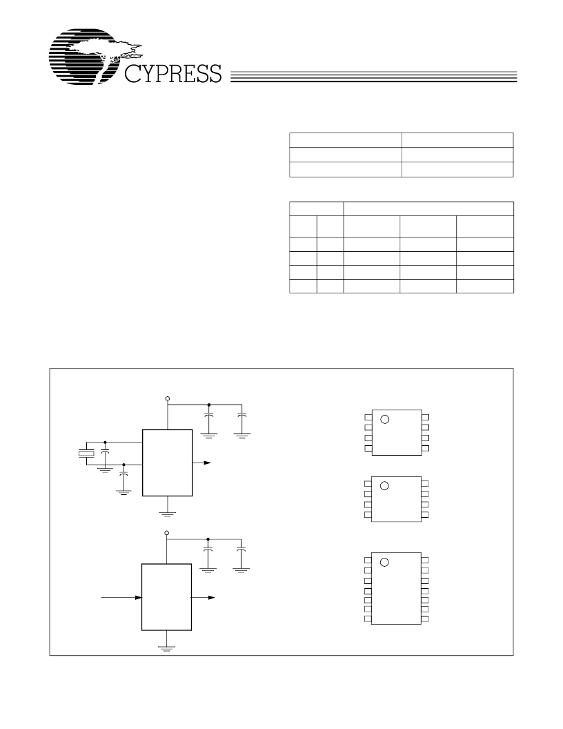
Simplified Block Diagram
Pin Configurations
W
8
7
6
5
1
2
3
4
CLKIN or X1
NC or X2
GND
SS%
SSON#
FS1
VDD
CLKOUT
W
8
7
6
5
1
2
3
4
CLKIN or X1
NC or X2
GND
SS%
FS2
FS1
VDD
CLKOUT
SOIC
Spread Spectrum
Output
W181
(EMI suppressed)
3.3 or 5.0V
Oscillator or
Reference Input
Spread Spectrum
Output
W181
(EMI suppressed)
3.3 or 5.0V
XTAL
Input
X1
X2
40 MHz
Max.
W
8
1
2
3
4
5
6
7
CLKIN or X1
NC or X2
GND
NC
SS%
NC
NC
NC
FS1
NC
VDD
NC
CLKOUT
9
10
11
12
13
14
FS2
TSSOP
相关PDF资料 |
PDF描述 |
|---|---|
| W182G | MISCELLANEOUS CLOCK GENERATOR|CMOS|SOP|14PIN|PLASTIC |
| W183G | MISCELLANEOUS CLOCK GENERATOR|CMOS|SOP|14PIN|PLASTIC |
| W184H | MISCELLANEOUS CLOCK GENERATOR|CMOS|SSOP|24PIN|PLASTIC |
| W185H | Miscellaneous Clock Generator |
| W185-5 | Six Output Peak Reducing EMI Solution |
相关代理商/技术参数 |
参数描述 |
|---|---|
| W181-03GI | 制造商:Rochester Electronics LLC 功能描述:- Bulk |
| W181-03GT | 制造商:Cypress Semiconductor 功能描述:PLL Frequency Synthesizer Single 8-Pin SOIC T/R |
| W18151G | 制造商:Cypress Semiconductor 功能描述: |
| W181-51G | 制造商:Cypress Semiconductor 功能描述:PLL Frequency Synthesizer Single 8-Pin SOIC |
| W181-51GT | 制造商:Cypress Semiconductor 功能描述:PLL Frequency Synthesizer Single 8-Pin SOIC T/R |
发布紧急采购,3分钟左右您将得到回复。