- 您现在的位置:买卖IC网 > PDF目录361766 > W185H Miscellaneous Clock Generator PDF资料下载
参数资料
| 型号: | W185H |
| 英文描述: | Miscellaneous Clock Generator |
| 中文描述: | 杂项时钟发生器 |
| 文件页数: | 1/8页 |
| 文件大小: | 116K |
| 代理商: | W185H |
Six Output Peak Reducing EMI Solution
W185
Cypress Semiconductor Corporation
3901 North First Street
San Jose
CA 95134
408-943-2600
July 25, 2000, rev. *A
Features
Cypress PREMIS
family offering
Generates an EMI optimized clocking signal at the
output
Selectable output frequency range
Six 1.25%, 3.75%, or 0% down or center spread outputs
One non-Spread output of Reference input
Integrated loop filter components
Operates with a 3.3V or 5V supply
Low power CMOS design
Available in 24-pin SSOP (Shrink Small Outline
Package)
Outputs may be selectively disabled
Key Specifications
Supply Voltages: ...........................................V
DD
= 3.3V±5%
or V
DD
= 5V±10%
Frequency Range: ............................ 28 MHz
≤
F
in
≤
75 MHz
Crystal Reference Range:................. 28 MHz
≤
F
in
≤
40 MHz
Cycle to Cycle Jitter: ....................................... 300 ps (max.)
Selectable Spread Percentage: ....................1.25% or 3.75%
Output Duty Cycle: ............................... 40/60% (worst case)
Output Rise and Fall Time: ..................................5 ns (max.)
Table 1. Modulation Width Selection
SS%
W185
Output
W185-5
Output
0
F
in
≥
F
out
≥
F
in
– 1.25%
F
in
+ 0.625%
≥
F
in
≥
– 0.625%
1
F
in
≥
F
out
≥
F
in
– 3.75%
F
in
+ 1.875%
≥
F
in
≥
–1.875%
Table 2. Frequency Range Selection
FS2
FS1
Frequency Range
0
0
28 MHz
≤
F
IN
≤
38 MHz
38 MHz
≤
F
IN
≤
48 MHz
46 MHz
≤
F
IN
≤
60 MHz
58 MHz
≤
F
IN
≤
75 MHz
0
1
1
0
1
1
Table 3. Output Enable
EN1
EN2
CLK0:4
CLK5
0
0
Low
Low
0
1
Low
Active
1
0
Active
Low
1
1
Active
Active
PREMIS is a trademark of Cypress Semiconductor Corporation.
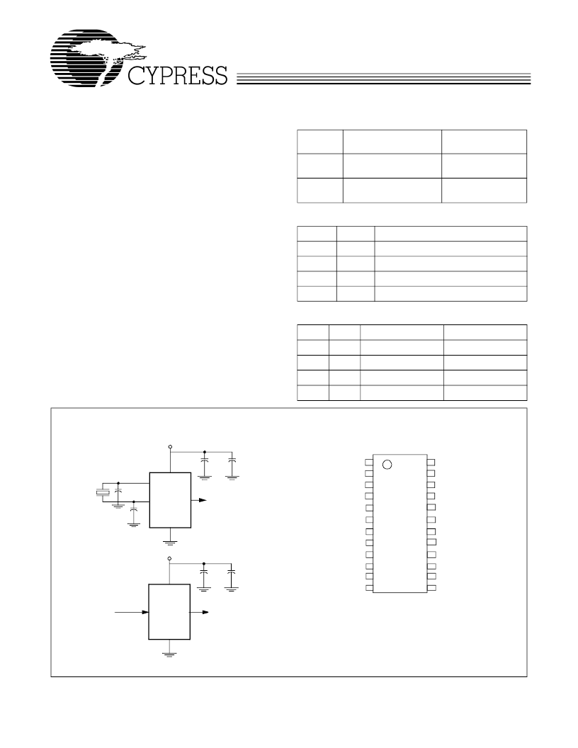
Simplified Block Diagram
Pin Configuration
W
24
23
22
21
20
1
2
3
4
5
6
7
8
9
10
11
12
REFOUT
FS2
X1
X2
GND
SS%
EN2
GND
CLK0
VDD
CLK1
CLK2
SSON#
RESET
FS1
VDD
VDD
NC
EN1
CLK5
VDD
CLK4
GND
CLK3
18
17
19
15
14
16
13
SSOP
Spread Spectrum
Output
W185
(EMI suppressed)
3.3V or 5.0V
Oscillator or
Reference Input
Spread Spectrum
W185
(EOutput
3.3V or 5.0V
XTAL
40MHz
max.
X1
X2
相关PDF资料 |
PDF描述 |
|---|---|
| W185-5 | Six Output Peak Reducing EMI Solution |
| W18NB40 | N-CHANNEL 400V - 0.19ohm - 18.4A TO-247/ISOWATT218 PowerMESH MOSFET |
| W191 | Clocks and Buffers |
| W194-70G | Miscellaneous Clock Generator |
| W195 | Clocks and Buffers |
相关代理商/技术参数 |
参数描述 |
|---|---|
| W185HT | 制造商:Cypress Semiconductor 功能描述: |
| W1869X2 | 制造商:n/a 功能描述:Ships in 2 days |
| W1869X6 | 制造商:n/a 功能描述:Ships in 2 days |
| W186E13 | 制造商:OMRON INDUSTRIAL AUTOMATION 功能描述:C500-ASC04 ASC11 Unit Op.Man. DX CODE ZA |
| W186E14 | 制造商:Omron Corporation 功能描述: |
发布紧急采购,3分钟左右您将得到回复。