- 您现在的位置:买卖IC网 > PDF目录22241 > W25X10AVSNIG (Winbond Electronics)IC FLASH 16MBIT 100MHZ 8SOIC PDF资料下载
参数资料
| 型号: | W25X10AVSNIG |
| 厂商: | Winbond Electronics |
| 文件页数: | 18/45页 |
| 文件大小: | 0K |
| 描述: | IC FLASH 16MBIT 100MHZ 8SOIC |
| 标准包装: | 100 |
| 系列: | SpiFlash® |
| 格式 - 存储器: | 闪存 |
| 存储器类型: | FLASH |
| 存储容量: | 1M (128K x 8) |
| 速度: | 100MHz |
| 接口: | SPI 串行 |
| 电源电压: | 2.7 V ~ 3.6 V |
| 工作温度: | -40°C ~ 85°C |
| 封装/外壳: | 8-SOIC(0.154",3.90mm 宽) |
| 供应商设备封装: | 8-SOIC |
| 包装: | 管件 |
第1页第2页第3页第4页第5页第6页第7页第8页第9页第10页第11页第12页第13页第14页第15页第16页第17页当前第18页第19页第20页第21页第22页第23页第24页第25页第26页第27页第28页第29页第30页第31页第32页第33页第34页第35页第36页第37页第38页第39页第40页第41页第42页第43页第44页第45页
�� �
�
�W25X10A,� W25X20A,� W25X40A,� W25X80A�
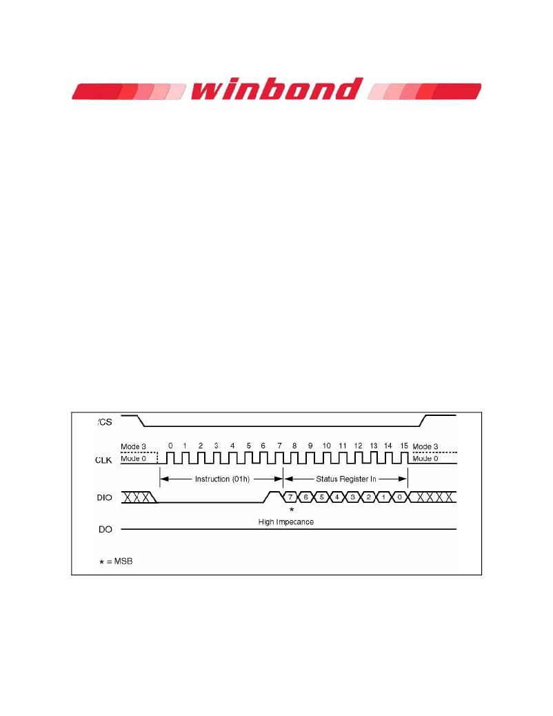
�10.2.6� Write� Status� Register� (01h)�
�The� Write� Status� Register� instruction� allows� the� Status� Register� to� be� written.� A� Write� Enable�
�instruction� must� previously� have� been� executed� for� the� device� to� accept� the� Write� Status� Register�
�Instruction� (Status� Register� bit� WEL� must� equal� 1).� Once� write� enabled,� the� instruction� is� entered� by�
�driving� /CS� low,� sending� the� instruction� code� “01h”,� and� then� writing� the� status� register� data� byte� as�
�illustrated� in� figure� 7.� The� Status� Register� bits� are� shown� in� figure� 3� and� described� earlier� in� this�
�datasheet.�
�Only� non-volatile� Status� Register� bits� SRP,� TB,� BP2,� BP1� and� BP0� (bits� 7,� 5,� 4,� 3� and� 2)� can� be�
�written� to.� All� other� Status� Register� bit� locations� are� read-only� and� will� not� be� affected� by� the� Write�
�Status� Register� instruction.�
�The� /CS� pin� must� be� driven� high� after� the� eighth� bit� of� the� last� byte� has� been� latched.� If� this� is� not�
�done� the� Write� Status� Register� instruction� will� not� be� executed.� After� /CS� is� driven� high,� the� self-timed�
�Write� Status� Register� cycle� will� commence� for� a� time� duration� of� t� W� (See� AC� Characteristics).� While�
�the� Write� Status� Register� cycle� is� in� progress,� the� Read� Status� Register� instruction� may� still� accessed�
�to� check� the� status� of� the� BUSY� bit.� The� BUSY� bit� is� a� 1� during� the� Write� Status� Register� cycle� and� a�
�0� when� the� cycle� is� finished� and� ready� to� accept� other� instructions� again.� After� the� Write� Register�
�cycle� has� finished� the� Write� Enable� Latch� (WEL)� bit� in� the� Status� Register� will� be� cleared� to� 0.�
�The� Write� Status� Register� instruction� allows� the� Block� Protect� bits� (TB,� BP2,� BP1� and� BP0)� to� be� set�
�for� protecting� all,� a� portion,� or� none� of� the� memory� from� erase� and� program� instructions.� Protected�
�areas� become� read-only� (see� Status� Register� Memory� Protection� table).� The� Write� Status� Register�
�instruction� also� allows� the� Status� Register� Protect� bit� (SRP)� to� be� set.� This� bit� is� used� in� conjunction�
�with� the� Write� Protect� (/WP)� pin� to� disable� writes� to� the� status� register.� When� the� SRP� bit� is� set� to� a� 0�
�state� (factory� default)� the� /WP� pin� has� no� control� over� the� status� register.� When� the� SRP� pin� is� set� to� a�
�1,� the� Write� Status� Register� instruction� is� locked� out� while� the� /WP� pin� is� low.� When� the� /WP� pin� is�
�high� the� Write� Status� Register� instruction� is� allowed.�
�Figure� 7.� Write� Status� Register� Instruction� Sequence� Diagram�
�-� 18� -�
�相关PDF资料 |
PDF描述 |
|---|---|
| EBM15DCAH | CONN EDGECARD 30POS R/A .156 SLD |
| VJ0805D201KXPAJ | CAP CER 200PF 250V 10% NP0 0805 |
| WSU090-0800 | POWER SUPPLY 100-240V 800MA |
| 395-130-527-802 | CARD EDGE 130PS DL .100X.200 BLK |
| VE-J0N-CX-F1 | CONVERTER MOD DC/DC 18.5V 75W |
相关代理商/技术参数 |
参数描述 |
|---|---|
| W25X10AVZPIG | 制造商:WINBOND 制造商全称:Winbond 功能描述:1M-BIT, 2M-BIT, 4M-BIT AND 8M-BIT SERIAL FLASH MEMORY WITH 4KB SECTORS AND DUAL OUTPUT SPI |
| W25X10BL | 制造商:WINBOND 制造商全称:Winbond 功能描述:1M-BIT, 2M-BIT AND 4M-BIT 2.5V SERIAL FLASH MEMORY WITH 4KB SECTORS AND DUAL I/O SPI |
| W25X10BLSNIG | 制造商:WINBOND 制造商全称:Winbond 功能描述:1M-BIT, 2M-BIT AND 4M-BIT 2.5V SERIAL FLASH MEMORY WITH 4KB SECTORS AND DUAL I/O SPI |
| W25X10BLZPIG | 制造商:WINBOND 制造商全称:Winbond 功能描述:1M-BIT, 2M-BIT AND 4M-BIT 2.5V SERIAL FLASH MEMORY WITH 4KB SECTORS AND DUAL I/O SPI |
| W25X10BV | 制造商:WINBOND 制造商全称:Winbond 功能描述:1M-BIT, 2M-BIT AND 4M-BIT SERIAL FLASH MEMORY WITH 4KB SECTORS AND DUAL I/O SPI |
发布紧急采购,3分钟左右您将得到回复。