- 您现在的位置:买卖IC网 > PDF目录68746 > W33D2031 (WINBOND ELECTRONICS CORP) LIQUID CRYSTAL DISPLAY DRIVER, PQFP64 PDF资料下载
参数资料
| 型号: | W33D2031 |
| 厂商: | WINBOND ELECTRONICS CORP |
| 元件分类: | 显示驱动器 |
| 英文描述: | LIQUID CRYSTAL DISPLAY DRIVER, PQFP64 |
| 封装: | PLASTIC, QFP-64 |
| 文件页数: | 23/28页 |
| 文件大小: | 305K |
| 代理商: | W33D2031 |
第1页第2页第3页第4页第5页第6页第7页第8页第9页第10页第11页第12页第13页第14页第15页第16页第17页第18页第19页第20页第21页第22页当前第23页第24页第25页第26页第27页第28页
W33D0001 SERIES
- 4 -
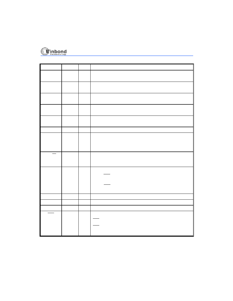
Pin Description, continued
SYMBOL
PIN
I/O
FUNCTION
COM1
COM4
56
59
O
LCD panel common pins.
(1/3 bias, 1/4 duty)
SEG1
SEG32
60
64,
2
28
O
LCD panel segment pins.
(1/3 bias, 1/4 duty)
RDATA
44
O
Serial data output pin. It is H-Z when not active.
Power source: VDD1
RCLK
42
I
Synchronous read clock input pin.
Power source: VDD1
WDATA
45
I
Serial data/address input pin.
Power source: VDD1
WCLK
41
I
Synchronous write clock input pin. Power source: VDD1
MS
43
I
Mode select input pin with floating status.
Normal mode is active high or low by mask option. MS pin is high
as normal mode through all the SPEC. Power source: VDD1
(Refer to functional description for more details)
12 / 24
47
I
12-hour (high) or 24-hour (low) clock select pin with floating
status.
Power source: VDD1
WFG
48
O
Waveform generator output pin.
When RST = 0, 1 Hz or 1024 Hz (selected by mask option) will
output from this pin.
When RST = 1, the control bits (248, 249, 250) will output the
square-wave from this pin. Power source: VDD1.
TIM
39
I
Timer start/stop control pin with floating status.
MODE
30
I
Clock mode-adjust pin with internal pull-low resistor.
SET
31
I
Clock digit-adjust pin with internal pull-low resistor.
ATS
49
I
Auto Timer Select pin with floating status.
ATS = 1, Auto timer disable.
ATS = 0, Auto timer enable.
(Refer to functional description for more details)
相关PDF资料 |
PDF描述 |
|---|---|
| W33D2041 | LIQUID CRYSTAL DISPLAY DRIVER, PQFP64 |
| W33D2111 | LIQUID CRYSTAL DISPLAY DRIVER, PQFP64 |
| W33D2121 | LIQUID CRYSTAL DISPLAY DRIVER, PQFP64 |
| W33D2131 | LIQUID CRYSTAL DISPLAY DRIVER, PQFP64 |
| W33D2141 | LIQUID CRYSTAL DISPLAY DRIVER, PQFP64 |
相关代理商/技术参数 |
参数描述 |
|---|---|
| W33-D3B1Q-20 | 制造商:TE Connectivity 功能描述: |
| W33FX-22 | 制造商:Magnecraft 功能描述: |
| W33HSX-178 | 制造商:Struthers-Dunn 功能描述: |
| W33HSX-179 | 制造商:Struthers-Dunn 功能描述: |
| W33HSX-182 | 制造商:Struthers-Dunn 功能描述: |
发布紧急采购,3分钟左右您将得到回复。