- 您现在的位置:买卖IC网 > PDF目录363887 > W48C111-16 (Cypress Semiconductor Corp.) Frequency Generator for Integrated Core Logic(在集成核心逻辑中应用的频率发生器) PDF资料下载
参数资料
| 型号: | W48C111-16 |
| 厂商: | Cypress Semiconductor Corp. |
| 英文描述: | Frequency Generator for Integrated Core Logic(在集成核心逻辑中应用的频率发生器) |
| 中文描述: | 频率发生器集成的核心逻辑(在集成核心逻辑中应用的频率发生器) |
| 文件页数: | 2/7页 |
| 文件大小: | 114K |
| 代理商: | W48C111-16 |
W48C111-16
PRELIMINARY
2
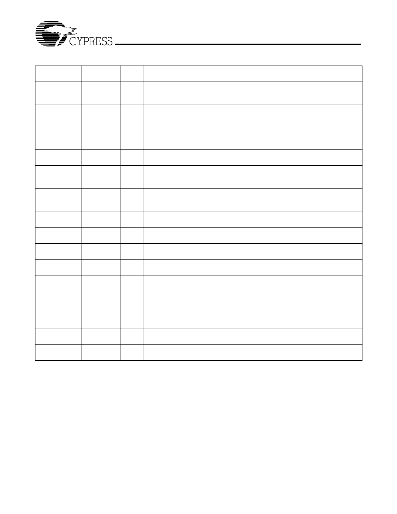
Pin Definitions
Pin Name
CPU0:1
Pin
No.
24, 23
Pin
Type
O
Pin Description
CPU Clock Outputs 0 and 1:
These two CPU clock outputs are controlled by the
CPU_STOP# control pin. Output voltage swing is controlled by voltage applied to
VDDQ2.
PCI1:5
5, 7, 8, 10,
11
O
PCI Bus Clock Outputs 1 through 5:
These five PCI clock outputs are controlled
by the PCI_STOP# control pin. Output voltage swing is controlled by voltage applied
to VDDQ3.
PCI_F
4
O
Fixed PCI Clock Output:
Unlike PCI1:5 outputs, this output is not controlled by the
PCI_STOP# control pin; it cannot be forced LOW by PCI_STOP#. Output voltage
swing is controlled by voltage applied to VDDQ3.
48MHz
16
O
48-MHz Output:
Fixed clock output at 48 MHz. Output voltage swing is controlled by
voltage applied to VDDQ3. This output does not have the SS feature
CPU_STOP#
18
I
CPU_STOP# input:
When brought LOW, clock outputs CPU0:1 are stopped LOW
after completing a full clock cycle (2
–
3 CPU clock latency). When brought HIGH,
clock outputs CPU0:1 start with a full clock cycle (2
–
3 CPU clock latency).
PCI_STOP#
19
I
PCI_STOP# input:
The PCI_STOP# input enables the PCI1:5 outputs when HIGH
and causes them to remain at logic 0 when LOW. The PCI_STOP signal is latched
on the rising edge of PCI_F. Its effect takes place on the next PCI_F clock cycle.
Fixed 14.318-MHz Output:
Used for various system applications. Output voltage
swing is controlled by voltage applied to VDDQ3.
REF
26
O
SEL100/66#
15
I
Frequency Selection Inputs:
Select power-up default CPU clock frequency as
shown in
Table 1
on page 1.
X1
1
I
Crystal Connection or External Reference Frequency Input:
This pin can either
be used as a connection to a crystal or to a reference signal.
X2
2
I
Crystal Connection:
An input connection for an external 14.318-MHz crystal. If
using an external reference, this pin must be left unconnected.
Power-Down Control:
When this input is LOW, device goes into a low-power stand-
by condition. All outputs are held LOW. CPU and PCI clock outputs are stopped LOW
after completing a full clock cycle (2
–
3 CPU clock cycle latency). When brought
HIGH, CPU and PCI outputs start with a full clock cycle at full operating frequency
(3 ms maximum latency).
Power Connection:
Connected to 3.3V supply.
PWR_DWN#
17
I
VDDQ3
6, 9, 13, 21,
27
P
VDDQ2
25
P
Power Connection:
Power supply for CPU0:1 output buffer. Connected to 2.5V or
3.3V.
GND
3, 12, 14, 20,
22, 28
G
Ground Connection:
Connect all ground pins to the common system ground plane.
相关PDF资料 |
PDF描述 |
|---|---|
| W48C111-17 | 100-MHz Mobile Motherboard System Clock(100-MHz 移动主板系统时钟) |
| W48C111 | Frequency Generator for Integrated Core Logic |
| W48C20 | Audio Subsystem Clock Generator(音频子系统时钟发生器) |
| W48C55A | Frequency Synthesizers(频率合成器) |
| W48C54A | Frequency Synthesizers(频率合成器) |
相关代理商/技术参数 |
参数描述 |
|---|---|
| W48C111-16H | 功能描述:IC CLOCK GEN FREQ MOD 28-SSOP RoHS:否 类别:集成电路 (IC) >> 时钟/计时 - 时钟发生器,PLL,频率合成器 系列:- 标准包装:1,000 系列:Precision Edge® 类型:时钟/频率合成器 PLL:无 输入:CML,PECL 输出:CML 电路数:1 比率 - 输入:输出:2:1 差分 - 输入:输出:是/是 频率 - 最大:10.7GHz 除法器/乘法器:无/无 电源电压:2.375 V ~ 3.6 V 工作温度:-40°C ~ 85°C 安装类型:表面贴装 封装/外壳:16-VFQFN 裸露焊盘,16-MLF? 供应商设备封装:16-MLF?(3x3) 包装:带卷 (TR) 其它名称:SY58052UMGTRSY58052UMGTR-ND |
| W48C111-16HT | 制造商:Rochester Electronics LLC 功能描述:- Tape and Reel |
| W48C111-17 | 制造商:CYPRESS 制造商全称:Cypress Semiconductor 功能描述:100-MHz Mobile Motherboard System Clock |
| W48C20 | 制造商:CYPRESS 制造商全称:Cypress Semiconductor 功能描述:Audio Subsystem Clock Generator |
| W48C20-08G | 制造商:未知厂家 制造商全称:未知厂家 功能描述:Miscellaneous Clock Generator |
发布紧急采购,3分钟左右您将得到回复。