- 您现在的位置:买卖IC网 > PDF目录276884 > W49F002UT12BN (WINBOND ELECTRONICS CORP) 256K X 8 FLASH 5V PROM, 120 ns, PDSO32 PDF资料下载
参数资料
| 型号: | W49F002UT12BN |
| 厂商: | WINBOND ELECTRONICS CORP |
| 元件分类: | PROM |
| 英文描述: | 256K X 8 FLASH 5V PROM, 120 ns, PDSO32 |
| 封装: | 8 X 20 MM, TSOP-32 |
| 文件页数: | 2/30页 |
| 文件大小: | 0K |
| 代理商: | W49F002UT12BN |
第1页当前第2页第3页第4页第5页第6页第7页第8页第9页第10页第11页第12页第13页第14页第15页第16页第17页第18页第19页第20页第21页第22页第23页第24页第25页第26页第27页第28页第29页第30页
W49F002U
- 10 -
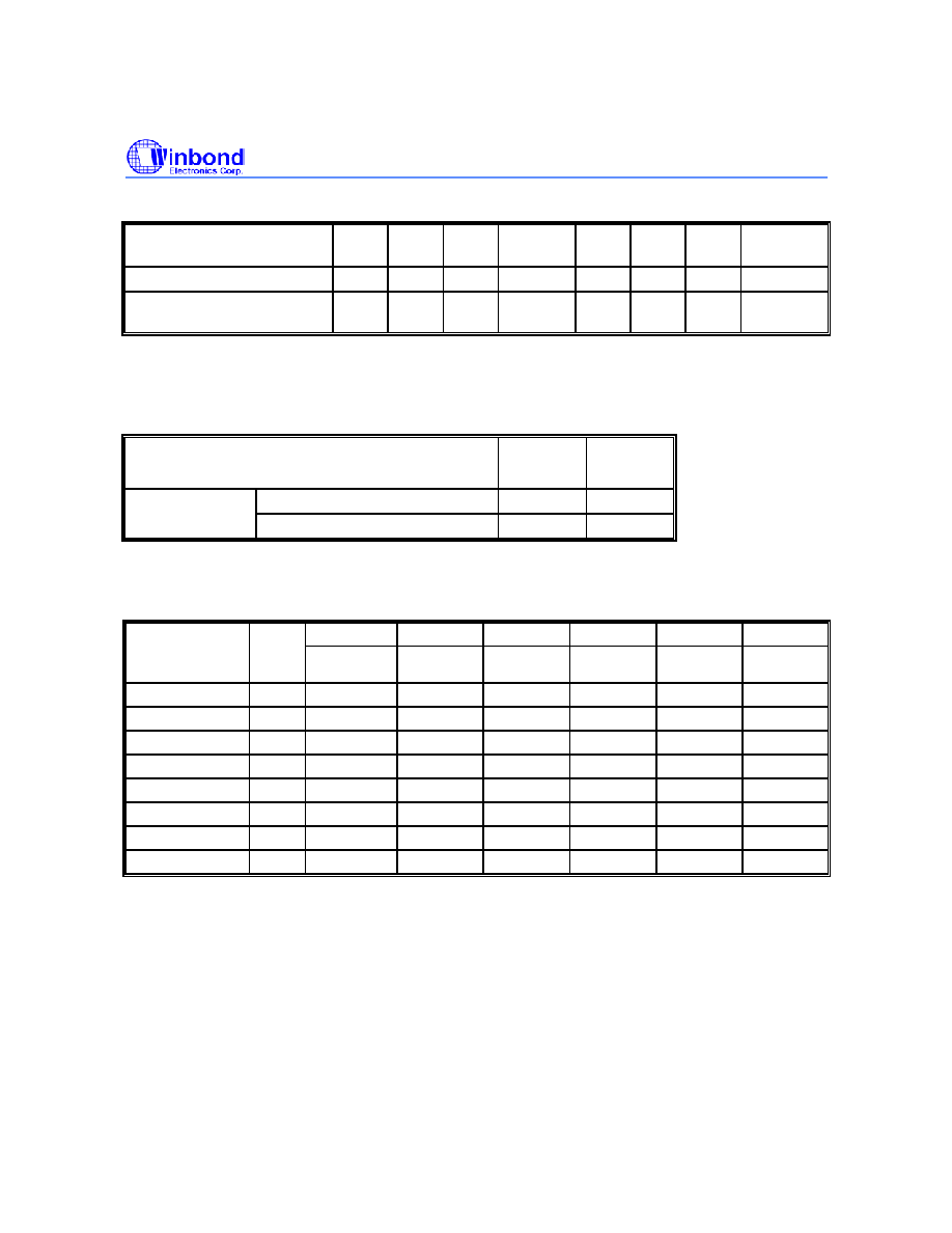
7.2 Auto-select Codes (High Voltage Method)
DESCRIPTION
#CE
#OE
#WE
OTHER
ADD
A9
A1
A0
DQ7
TO DQ0
Manufacturer ID: Winbond
VIL
VIH
X
VID
VIL
DAh
Device ID: W49F002U
(Top Boot Block)
VIL
VIH
X
VID
VIL
VIH
0Bh
Notes:
1. SA = Sector Address, X = Don
′t Care. Sector Protection Verification: 01h (protected); 00h (unprotected).
2. The hardware SID read function is not included in all parts; please refer to Ordering Information for details.
Hardware Sequence Flags
OPERATION
DQ7
(NOTE)
DQ6
Embedded Program Algorithm
#DQ7
Toggle
Standard Mode
Embedded Erase Algorithm
0
Toggle
Note: DQ7 require a valid address when reading status information. Refer to the appropriate subsection for further details.
Command Definition(1)
1TH CYCLE
2ND CYCLE
3RD CYCLE
4TH CYCLE
5TH CYCLE
6TH CYCLE
COMMAND
DESCRIPTION
NO. OF
CYCLES
ADDR. DATA
ADDR.
DATA
ADDR.
DATA
ADDR.
DATA
ADDR.
DATA
ADDR.
DATA
Read
1
AIN DOUT
Chip Erase
6
5555 AA
2AAA 55
5555 80
5555 AA
2AAA 55
5555 10
Sector Erase
6
5555 AA
2AAA 55
5555 80
5555 AA
2AAA 55
SA
(3)
30
Byte Program
4
5555 AA
2AAA 55
5555 A0
AIN DIN
Boot Block Lockout
6
5555 AA
2AAA 55
5555 80
5555 AA
2AAA 55
5555 40
Product ID Entry
3
5555 AA
2AAA 55
5555 90
Product ID Exit (2)
3
5555 AA
2AAA 55
5555 F0
Product ID Exit (2)
1
XXXX F0
Notes:
1. Address Format: A14
A0 (Hex); Data Format: DQ7 DQ0 (Hex)
2. Either one of the two Product ID Exit commands can be used.
3. SA means: Sector Address
If SA is within 3C000 to 3FFFF (Boot Block address range), and the Boot Block programming lockout feature is activated,
nothing will happen and the device will go back to read mode after 100nS.
If the Boot Block programming lockout feature is not activated, this command will erase Boot Block.
If SA is within 3A000 to 3BFFF (Parameter Block1 address range), this command will erase PB1.
If SA is within 38000 to 39FFF (Parameter Block2 address range), this command will erase PB2.
If SA is within 20000 to 37FFF (Main Memory Block1 address range), this command will erase MMB1.
If SA is within 00000 to 1FFFF (Main Memory Block2 address range), this command will erase MMB2.
相关PDF资料 |
PDF描述 |
|---|---|
| W3EG72255S202D3M | 256M X 72 DDR DRAM MODULE, 0.8 ns, DMA184 |
| W3EG72255S263D3M | 256M X 72 DDR DRAM MODULE, 0.75 ns, DMA184 |
| W7NCF512H10CSA3HM1G | FLASH 3.3V PROM MODULE, XMA50 |
| W7NCF512H10CSA6BM1G | FLASH 3.3V PROM MODULE, XMA50 |
| W7NCF512H10CSABEM1G | FLASH 3.3V PROM MODULE, XMA50 |
相关代理商/技术参数 |
参数描述 |
|---|---|
| W49F002UT70B | 制造商:WINBOND 制造商全称:Winbond 功能描述:256K X 8 CMOS FLASH MEMORY |
| W49F002UT90B | 制造商:WINBOND 制造商全称:Winbond 功能描述:256K X 8 CMOS FLASH MEMORY |
| W49F020 | 制造商:WINBOND 制造商全称:Winbond 功能描述:256K X 8 CMOS FLASH MEMORY |
| W49F020-70 | 制造商:WINBOND 制造商全称:Winbond 功能描述:256K X 8 CMOS FLASH MEMORY |
| W49F020-70B | 制造商:WINBOND 制造商全称:Winbond 功能描述:256K X 8 CMOS FLASH MEMORY |
发布紧急采购,3分钟左右您将得到回复。