- 您现在的位置:买卖IC网 > PDF目录231499 > WSF128K32-22H2M (WHITE ELECTRONIC DESIGNS CORP) SPECIALTY MEMORY CIRCUIT, CPGA66 PDF资料下载
参数资料
| 型号: | WSF128K32-22H2M |
| 厂商: | WHITE ELECTRONIC DESIGNS CORP |
| 元件分类: | 存储器 |
| 英文描述: | SPECIALTY MEMORY CIRCUIT, CPGA66 |
| 封装: | CERAMIC, HIP-66 |
| 文件页数: | 1/12页 |
| 文件大小: | 505K |
| 代理商: | WSF128K32-22H2M |
1
White Electronic Designs Corporation (602) 437-1520 www.whiteedc.com
White Electronic Designs
WSF128K32-XH2X
October 2004
Rev. 4
White Electronic Designs Corp. reserves the right to change products or specications without notice.
PRELIMINARY*
128KX32 SRAM/FLASH MODULE
FEATURES
Access Times of 25ns (SRAM) and 70, 90 and
120ns (FLASH)
Packaging:
66-pin, PGA Type, 1.385 inch square HIP,
Hermetic Ceramic HIP (Package 402)
128Kx32 SRAM
128Kx32 5V Flash
Organized as 128Kx32 of SRAM and 128Kx32 of
Flash Memory with common Data Bus
Low Power CMOS
Commercial, Industrial and Military Temperature
Ranges
TTL Compatible Inputs and Outputs
Built-in Decoupling Caps and Multiple Ground Pins
for Low Noise Operation
Weight - 13 grams typical
FLASH MEMORY FEATURES
10,000 Erase/Program Cycles
Sector Architecture
8 equal size sectors of 16K bytes each
Any combination of sectors can be concurrently
erased. Also supports full chip erase
5 Volt Programming; 5V ± 10% Supply
Embedded Erase and Program Algorithms
Hardware Write Protection
Page Program Operation and Internal Program
Control Time.
* This product is under development, not fully characterized, and is subject to change
without notice.
Note: Programming information available upon request.
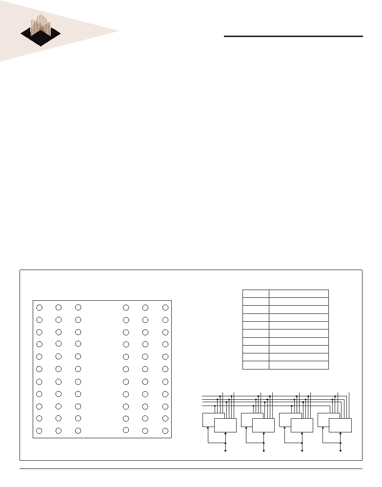
FIGURE 1 – PIN CONFIGURATION FOR WSF128K32-XH2X
Block Diagram
I/O8
I/O9
I/O10
A14
A16
A11
A0
NC
I/O0
I/O1
I/O2
FWE2#
SWE2#
GND
I/O11
A10
A9
A15
VCC
FCS#
SCS#
I/O3
I/O15
I/O14
I/O13
I/O12
OE#
NC
FWE1#
I/O7
I/O6
I/O5
I/O4
I/O24
I/O25
I/O26
A7
A12
SWE1#
A13
A8
I/O16
I/O17
I/O18
VCC
SWE4#
FWE4#
I/O27
A4
A5
A6
FWE3#
SWE3#
GND
I/O19
I/O31
I/O30
I/O29
I/O28
A1
A2
A3
I/O23
I/O22
I/O21
I/O20
11
22
33
44
55
66
1
12
23
34
45
56
Top View
OE#
FCS#
SCS#
A0-16
FWE1# SWE1#FWE2#SWE2#FWE3#SWE3#FWE4#SWE4#
128K x 8 Flash
128K x 8 SRAM
I/O0-7
128K x 8 Flash
128K x 8 SRAM
I/O8-15
128K x 8 Flash
128K x 8 SRAM
I/O16-23
128K x 8 Flash
128K x 8 SRAM
I/O24-31
Pin Description
D0-31
Data Inputs/Outputs
A0-16
Address Inputs
SWE1-4#
SRAM Write Enable
SCS#
SRAM Chip Selects
OE#
Output Enable
VCC
Power Supply
GND
Ground
NC
Not Connected
FWE1-4#
Flash Write Enable
FCS#
Flash Chip Select
相关PDF资料 |
PDF描述 |
|---|---|
| WS512K32N-35H2QA | 2M X 8 MULTI DEVICE SRAM MODULE, 35 ns, CPGA66 |
| WME128K8-250CIA | 128K X 8 EEPROM 5V, 250 ns, CDIP32 |
| WME128K8-300CMA | 128K X 8 EEPROM 5V, 300 ns, CDIP32 |
| WME128K8-300DEM | 128K X 8 EEPROM 5V, 300 ns, CDSO32 |
| WMS256K16-17FGCA | 256K X 16 STANDARD SRAM, 17 ns, CDSO44 |
相关代理商/技术参数 |
参数描述 |
|---|---|
| WSF128K32-22H2MA | 制造商:未知厂家 制造商全称:未知厂家 功能描述:128K x 32 SRAM/FLASH MODULE |
| WSF128K32-27H2C | 制造商:未知厂家 制造商全称:未知厂家 功能描述:128K x 32 SRAM/FLASH MODULE |
| WSF128K32-27H2CA | 制造商:WEDC 制造商全称:White Electronic Designs Corporation 功能描述:128KX32 SRAM/FLASH MODULE |
| WSF128K32-27H2I | 制造商:未知厂家 制造商全称:未知厂家 功能描述:128K x 32 SRAM/FLASH MODULE |
| WSF128K32-27H2IA | 制造商:未知厂家 制造商全称:未知厂家 功能描述:128K x 32 SRAM/FLASH MODULE |
发布紧急采购,3分钟左右您将得到回复。