参数资料
| 型号: | X1227S8IZ-4.5A |
| 厂商: | Intersil |
| 文件页数: | 11/28页 |
| 文件大小: | 0K |
| 描述: | IC RTC/CAL/CPU SUP EE 8-SOIC |
| 标准包装: | 100 |
| 类型: | 时钟/日历 |
| 特点: | 警报器,闰年,监控器,监视计时器 |
| 时间格式: | HH:MM:SS(12/24 小时) |
| 数据格式: | YY-MM-DD-dd |
| 接口: | I²C,2 线串口 |
| 电源电压: | 4.5 V ~ 5.5 V |
| 电压 - 电源,电池: | 1.8 V ~ 5.5 V |
| 工作温度: | -40°C ~ 85°C |
| 安装类型: | 表面贴装 |
| 封装/外壳: | 8-SOIC(0.154",3.90mm 宽) |
| 供应商设备封装: | 8-SOIC |
| 包装: | 管件 |
第1页第2页第3页第4页第5页第6页第7页第8页第9页第10页当前第11页第12页第13页第14页第15页第16页第17页第18页第19页第20页第21页第22页第23页第24页第25页第26页第27页第28页
19
FN8099.2
May 8, 2006
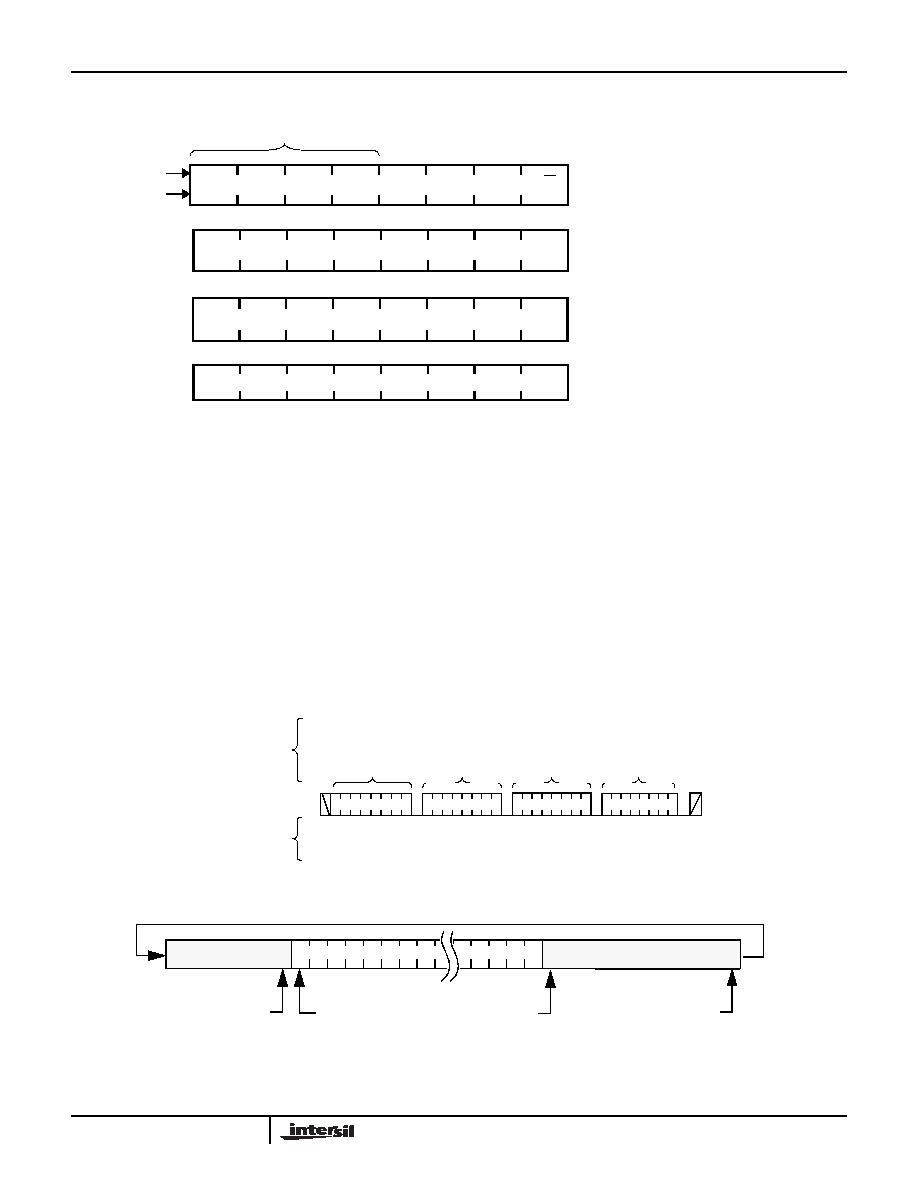
Figure 11. Slave Address, Word Address, and Data Bytes (64 Byte pages)
Write Operations
Byte Write
For a write operation, the device requires the Slave
Address Byte and the Word Address Bytes. This gives
the master access to any one of the words in the array
or CCR. (Note: Prior to writing to the CCR, the master
must write a 02h, then 06h to the status register in two
preceding operations to enable the write operation.
See “Writing to the Clock/Control Registers.” Upon
receipt of each address byte, the X1227 responds with
an acknowledge. After receiving both address bytes
the X1227 awaits the eight bits of data. After receiving
the 8 data bits, the X1227 again responds with an
acknowledge. The master then terminates the transfer
by generating a stop condition. The X1227 then
begins an internal write cycle of the data to the nonvol-
atile memory. During the internal write cycle, the
device inputs are disabled, so the device will not
respond to any requests from the master. The SDA out-
put is at high impedance. See Figure 12.
A write to a protected block of memory is ignored, but
will still receive an acknowledge. At the end of the
write command, the X1227 will not initiate an internal
write cycle, and will continue to ACK commands.
Figure 12. Byte Write Sequence
Figure 13. Writing 30 bytes to a 64-byte memory page starting at address 40.
Slave Address Byte
Byte 0
D7
D6
D5
D2
D4
D3
D1
D0
A0
A7
A2
A4
A3
A1
Data Byte
Byte 3
A6
A5
00
0
A8
0
1
0
1
0
1
0
1
R/W
1
Device Identifier
Array
CCR
0
Word Address 1
Byte 1
Word Address 0
Byte 2
S
t
a
r
t
S
t
o
p
Slave
Address
Word
Address 1
Data
A
C
K
A
C
K
A
C
K
SDA Bus
Signals From
The Slave
Signals from
the Master
0
A
C
K
Word
Address 0
1
0 000 00 0
Address
40
23 Bytes
63
7 Bytes
Address
= 6
Address Pointer
Ends Here
Addr = 7
X1227
相关PDF资料 |
PDF描述 |
|---|---|
| X1227S8IZ-2.7AT1 | IC RTC/CAL/CPU SUP EE 8-SOIC |
| MCP4252T-103E/UN | IC RHEOSTAT 10K 2CH 10-MSOP |
| MCP4252T-104E/MF | IC RHEOSTAT 100K 2CH 10-DFN |
| X1227S8IZ-2.7A | IC RTC/CAL/CPU SUP EE 8-SOIC |
| MCP4252T-104E/UN | IC RHEOSTAT 100K 2CH 10-MSOP |
相关代理商/技术参数 |
参数描述 |
|---|---|
| X1227S8T1 | 功能描述:IC RTC/CAL/CPU SUP EE 8-SOIC RoHS:否 类别:集成电路 (IC) >> 时钟/计时 - 实时时钟 系列:- 产品培训模块:Obsolescence Mitigation Program 标准包装:1 系列:- 类型:时钟/日历 特点:警报器,闰年,SRAM 存储容量:- 时间格式:HH:MM:SS(12/24 小时) 数据格式:YY-MM-DD-dd 接口:SPI 电源电压:2 V ~ 5.5 V 电压 - 电源,电池:- 工作温度:-40°C ~ 85°C 安装类型:表面贴装 封装/外壳:8-WDFN 裸露焊盘 供应商设备封装:8-TDFN EP 包装:管件 |
| X1227S8Z | 功能描述:IC RTC/CAL/CPU SUP EE 8-SOIC RoHS:是 类别:集成电路 (IC) >> 时钟/计时 - 实时时钟 系列:- 产品培训模块:Obsolescence Mitigation Program 标准包装:1 系列:- 类型:时钟/日历 特点:警报器,闰年,SRAM 存储容量:- 时间格式:HH:MM:SS(12/24 小时) 数据格式:YY-MM-DD-dd 接口:SPI 电源电压:2 V ~ 5.5 V 电压 - 电源,电池:- 工作温度:-40°C ~ 85°C 安装类型:表面贴装 封装/外壳:8-WDFN 裸露焊盘 供应商设备封装:8-TDFN EP 包装:管件 |
| X1227S8Z-2.7 | 功能描述:IC RTC/CAL/CPU SUP EE 8-SOIC RoHS:是 类别:集成电路 (IC) >> 时钟/计时 - 实时时钟 系列:- 产品培训模块:Obsolescence Mitigation Program 标准包装:1 系列:- 类型:时钟/日历 特点:警报器,闰年,SRAM 存储容量:- 时间格式:HH:MM:SS(12/24 小时) 数据格式:YY-MM-DD-dd 接口:SPI 电源电压:2 V ~ 5.5 V 电压 - 电源,电池:- 工作温度:-40°C ~ 85°C 安装类型:表面贴装 封装/外壳:8-WDFN 裸露焊盘 供应商设备封装:8-TDFN EP 包装:管件 |
| X1227S8Z-2.7A | 功能描述:IC RTC/CAL/CPU SUP EE 8-SOIC RoHS:是 类别:集成电路 (IC) >> 时钟/计时 - 实时时钟 系列:- 产品培训模块:Obsolescence Mitigation Program 标准包装:1 系列:- 类型:时钟/日历 特点:警报器,闰年,SRAM 存储容量:- 时间格式:HH:MM:SS(12/24 小时) 数据格式:YY-MM-DD-dd 接口:SPI 电源电压:2 V ~ 5.5 V 电压 - 电源,电池:- 工作温度:-40°C ~ 85°C 安装类型:表面贴装 封装/外壳:8-WDFN 裸露焊盘 供应商设备封装:8-TDFN EP 包装:管件 |
| X1227S8Z-4.5A | 功能描述:IC RTC/CAL/CPU SUP EE 8-SOIC RoHS:是 类别:集成电路 (IC) >> 时钟/计时 - 实时时钟 系列:- 产品培训模块:Obsolescence Mitigation Program 标准包装:1 系列:- 类型:时钟/日历 特点:警报器,闰年,SRAM 存储容量:- 时间格式:HH:MM:SS(12/24 小时) 数据格式:YY-MM-DD-dd 接口:SPI 电源电压:2 V ~ 5.5 V 电压 - 电源,电池:- 工作温度:-40°C ~ 85°C 安装类型:表面贴装 封装/外壳:8-WDFN 裸露焊盘 供应商设备封装:8-TDFN EP 包装:管件 |
发布紧急采购,3分钟左右您将得到回复。