参数资料
| 型号: | X1288V14I-2.7A |
| 厂商: | Intersil |
| 文件页数: | 27/27页 |
| 文件大小: | 0K |
| 描述: | IC RTC/CAL/CPU SUP EE 14-TSSOP |
| 标准包装: | 95 |
| 类型: | 时钟/日历 |
| 特点: | 警报器,闰年,监控器,监视计时器 |
| 时间格式: | HH:MM:SS:hh(12/24 小时) |
| 数据格式: | YY-MM-DD-dd |
| 接口: | I²C,2 线串口 |
| 电源电压: | 2.7 V ~ 5.5 V |
| 电压 - 电源,电池: | 1.8 V ~ 5.5 V |
| 工作温度: | -40°C ~ 85°C |
| 安装类型: | 表面贴装 |
| 封装/外壳: | 14-TSSOP(0.173",4.40mm 宽) |
| 供应商设备封装: | 14-TSSOP |
| 包装: | 管件 |
第1页第2页第3页第4页第5页第6页第7页第8页第9页第10页第11页第12页第13页第14页第15页第16页第17页第18页第19页第20页第21页第22页第23页第24页第25页第26页当前第27页
9
FN8102.3
April 14, 2006
The device offers a backup power input pin. This VBACK
pin allows the device to be backed up by battery or
SuperCap. The entire X1288 device is fully operational
from 2.7 to 5.5 volts and the clock/calendar portion of the
X1288 device remains fully operational down to 1.8 volts
(Standby Mode).
The X1288 device provides 256K bits of EEPROM with 8
modes of BlockLock control. The BlockLock allows a
safe, secure memory for critical user and configuration
data, while allowing a large user storage area.
PIN DESCRIPTIONS
Serial Clock (SCL)
The SCL input is used to clock all data into and out of the
device. The input buffer on this pin is always active (not
gated).
Serial Data (SDA)
SDA is a bidirectional pin used to transfer data into and
out of the device. It has an open drain output and may be
wire ORed with other open drain or open collector out-
puts. The input buffer is always active (not gated).
An open drain output requires the use of a pull-up resis-
tor. The output circuitry controls the fall time of the output
signal with the use of a slope controlled pull-down. The
circuit is designed for 400kHz 2-wire interface speed.
VBACK
This input provides a backup supply voltage to the
device. VBACK supplies power to the device in the event
the VCC supply fails. This pin can be connected to a bat-
tery, a Supercap or tied to ground if not used.
RESET Output – RESET
This is a reset signal output. This signal notifies a host
processor that the watchdog time period has expired or
that the voltage has dropped below a fixed VTRIP thresh-
old. It is an open drain active LOW output. Recom-
mended value for the pullup resistor is 5k
. If unused, tie
to ground.
Programmable Frequency/Interrupt Output – PHZ/IRQ
This is either an output from the internal oscillator or an
interrupt signal output. It is a CMOS output.
When used as frequency output, this signal has a fre-
quency of 32.768kHz, 100Hz, 1Hz or inactive.
When used as interrupt output, this signal notifies a host
processor that an alarm has occurred and an action is
required. It is an active LOW output.
The control bits for this function are FO1 and FO0 and
are found in address 0011h of the Clock Control Memory
X1, X2
The X1 and X2 pins are the input and output,
respectively, of an inverting amplifier. An external
32.768kHz quartz crystal is used with the X1288 to
supply a timebase for the real time clock. The
recommended crystal is a Citizen CFS206-32.768KDZF.
Internal compensation circuitry is included to form a
complete oscillator circuit. Care should be taken in the
placement of the crystal and the layout of the circuit.
Plenty of ground plane around the device and short
traces to X1 and X2 are highly recommended. See
Application section for more information.
POWER CONTROL OPERATION
The power control circuit accepts a VCC and a VBACK
input. The power control circuit powers the clock from
VBACK when VCC < VBACK - 0.2V. It will switch back to
power the device from VCC when VCC exceeds VBACK.
REAL TIME CLOCK OPERATION
The Real Time Clock (RTC) uses an external 32.768kHz
quartz crystal to maintain an accurate internal represen-
tation of the 1/100 of a second, second, minute, hour,
day, date, month, and year. The RTC has leap-year cor-
rection. The clock also corrects for months having fewer
than 31 days and has a bit that controls 24 hour or
AM/PM format. When the X1288 powers up after the loss
of both VCC and VBACK, the clock will not operate until at
least one byte is written to the clock register.
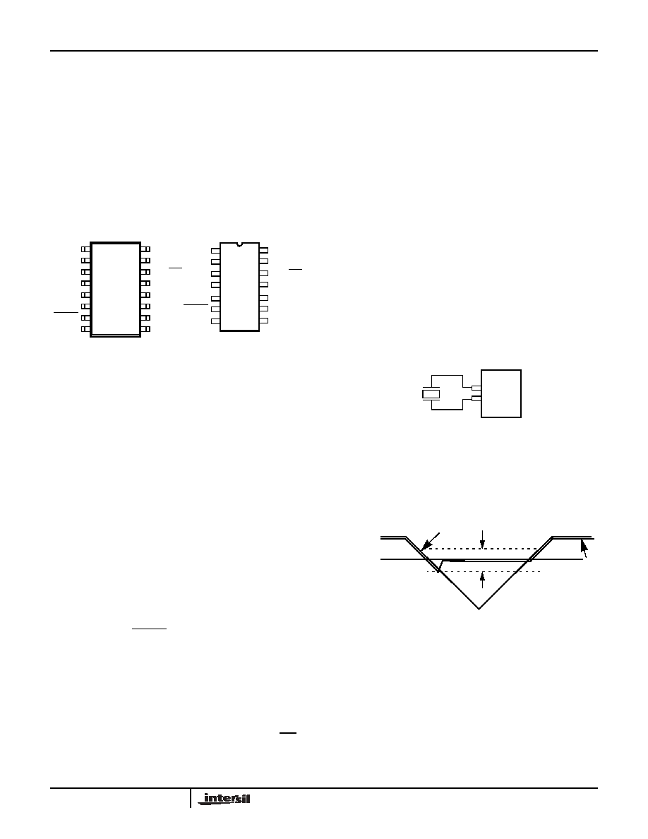
X1288
X1
X2
VBACK
VCC
NC
PHZ/IRQ
NC
VSS
1
2
3
4
13
14
12
11
14 Ld TSSOP
NC
SCL
NC
RESET
SDA
5
6
7
9
10
8
16 Ld SOIC
1
2
3
4
5
6
7
8
16
15
14
13
12
11
10
9
X1
X2
NC
VSS
NC
RESET
NC
VBACK
VCC
PHZ/IRQ
NC
SCL
NC
SDA
NC
NC = No internal connection
X1
X2
FIGURE 2. RECOMMENDED CRYSTAL CONNECTION
VBACK
In
Voltage
VCC
On
Off
FIGURE 3. POWER CONTROL
X1288
相关PDF资料 |
PDF描述 |
|---|---|
| MCP4161T-503E/MF | IC POT DGTL SNGL 50K SPI 8DFN |
| VE-B1M-MW-B1 | CONVERTER MOD DC/DC 10V 100W |
| X1288V14I-2.7 | IC RTC/CAL/CPU SUP EE 14-TSSOP |
| VE-21M-MW | CONVERTER MOD DC/DC 10V 100W |
| X1288V14I | IC RTC/CAL/CPU SUP EE 14-TSSOP |
相关代理商/技术参数 |
参数描述 |
|---|---|
| X1288V14I-4.5A | 功能描述:IC RTC/CAL/CPU SUP EE 14-TSSOP RoHS:否 类别:集成电路 (IC) >> 时钟/计时 - 实时时钟 系列:- 产品培训模块:Obsolescence Mitigation Program 标准包装:1 系列:- 类型:时钟/日历 特点:警报器,闰年,SRAM 存储容量:- 时间格式:HH:MM:SS(12/24 小时) 数据格式:YY-MM-DD-dd 接口:SPI 电源电压:2 V ~ 5.5 V 电压 - 电源,电池:- 工作温度:-40°C ~ 85°C 安装类型:表面贴装 封装/外壳:8-WDFN 裸露焊盘 供应商设备封装:8-TDFN EP 包装:管件 |
| X1288V14I-4.5AT1 | 功能描述:IC RTC/CAL/CPU SUP EE 14-TSSOP RoHS:否 类别:集成电路 (IC) >> 时钟/计时 - 实时时钟 系列:- 产品培训模块:Obsolescence Mitigation Program 标准包装:1 系列:- 类型:时钟/日历 特点:警报器,闰年,SRAM 存储容量:- 时间格式:HH:MM:SS(12/24 小时) 数据格式:YY-MM-DD-dd 接口:SPI 电源电压:2 V ~ 5.5 V 电压 - 电源,电池:- 工作温度:-40°C ~ 85°C 安装类型:表面贴装 封装/外壳:8-WDFN 裸露焊盘 供应商设备封装:8-TDFN EP 包装:管件 |
| X1288V14IT1 | 功能描述:IC RTC/CAL/CPU SUP EE 14-TSSOP RoHS:否 类别:集成电路 (IC) >> 时钟/计时 - 实时时钟 系列:- 产品培训模块:Obsolescence Mitigation Program 标准包装:1 系列:- 类型:时钟/日历 特点:警报器,闰年,SRAM 存储容量:- 时间格式:HH:MM:SS(12/24 小时) 数据格式:YY-MM-DD-dd 接口:SPI 电源电压:2 V ~ 5.5 V 电压 - 电源,电池:- 工作温度:-40°C ~ 85°C 安装类型:表面贴装 封装/外壳:8-WDFN 裸露焊盘 供应商设备封装:8-TDFN EP 包装:管件 |
| X1288V14IZ | 制造商:Rochester Electronics LLC 功能描述: 制造商:Intersil Corporation 功能描述: |
| X1288V14IZ-2.7 | 制造商:INTERSIL 制造商全称:Intersil Corporation 功能描述:2-Wire⑩ RTC Real Time Clock/Calendar/CPU Supervisor with EEPROM |
发布紧急采购,3分钟左右您将得到回复。