参数资料
| 型号: | X40410V8-B |
| 厂商: | Intersil |
| 文件页数: | 5/24页 |
| 文件大小: | 0K |
| 描述: | IC VOLTAGE MON DUAL W/SUP 8TSSOP |
| 标准包装: | 100 |
| 类型: | 多压监控器 |
| 监视电压数目: | 2 |
| 输出: | 开路漏极,推挽式 |
| 复位: | 高有效/低有效 |
| 复位超时: | 可调节/可选择 |
| 电压 - 阀值: | 2.6V,4.4V |
| 工作温度: | 0°C ~ 70°C |
| 安装类型: | 表面贴装 |
| 封装/外壳: | 8-TSSOP(0.173",4.40mm 宽) |
| 供应商设备封装: | 8-TSSOP |
| 包装: | 管件 |
�� �
�
�X40410,� X40411,� X40414,� X40415�
�Resetting� the� V� TRIPx� Voltage�
�To� reset� a� V� TRIPx� voltage,� apply� the� programming� volt-�
�age� (Vp)� to� the� WDO� pin� before� a� START� condition� is�
�set� up� on� SDA.� Next,� issue� on� the� SDA� pin� the� Slave�
�Address� A0h� followed� by� the� Byte� Address� 03h� for�
�V� TRIP1� and� 0Bh� for� V� TRIP2� ,� followed� by� 00h� for� the�
�Data� Byte� in� order� to� reset� V� TRIPx� .� The� STOP� bit� fol-�
�lowing� a� valid� write� operation� initiates� the� program-�
�ming� sequence.� Pin� WDO� must� then� be� brought� LOW�
�to� complete� the� operation.�
�After� being� reset,� the� value� of� V� TRIPx� becomes� a� nomi-�
�nal� value� of� 1.7V� or� lesser.�
�Note:� This� operation� does� not� corrupt� the� memory�
�array.�
�CONTROL� REGISTER�
�The� Control� Register� provides� the� user� a� mechanism� for�
�operation� directly� to� the� address� of� the� register� and� only�
�one� data� byte� is� allowed� for� each� register� write� operation.�
�Prior� to� writing� to� the� Control� Register,� the� WEL� and�
�RWEL� bits� must� be� set� using� a� two� step� process,� with�
�the� whole� sequence� requiring� 3� steps.� See� "Writing� to�
�the� Control� Registers"� on� page� 7.�
�The� user� must� issue� a� stop,� after� sending� this� byte� to�
�the� register,� to� initiate� the� nonvolatile� cycle� that� stores�
�WD1,� WD0,� PUP1,� PUP0,� BP1,� and� BP0.� The�
�X40410/11/14/15� will� not� acknowledge� any� data� bytes�
�written� after� the� first� byte� is� entered.�
�The� state� of� the� Control� Register� can� be� read� at� any�
�time� by� performing� a� random� read� at� address� 01Fh,�
�using� the� special� preamble.� Only� one� byte� is� read� by�
�each� register� read� operation.� The� master� should� sup-�
�ply� a� stop� condition� to� be� consistent� with� the� bus� pro-�
�tocol,� but� a� stop� is� not� required� to� end� this� operation.�
�changing� the� Block� Lock� and� Watchdog� Timer� settings.�
�7�
�6�
�5�
�4�
�3�
�2�
�1�
�0�
�The� Block� Lock� and� Watchdog� Timer� bits� are� nonvolatile�
�PUP1� WD1�
�WD0�
�BP�
�0�
�RWEL� WEL� PUP0�
�and� do� not� change� when� power� is� removed.�
�The� Control� Register� is� accessed� with� a� special� pream-�
�ble� in� the� slave� byte� (1011)� and� is� located� at� address�
�1FFh.� It� can� only� be� modified� by� performing� a� byte� write�
�RWEL:� Register� Write� Enable� Latch� (Volatile)�
�The� RWEL� bit� must� be� set� to� “1”� prior� to� a� write� to� the�
�Control� Register.�
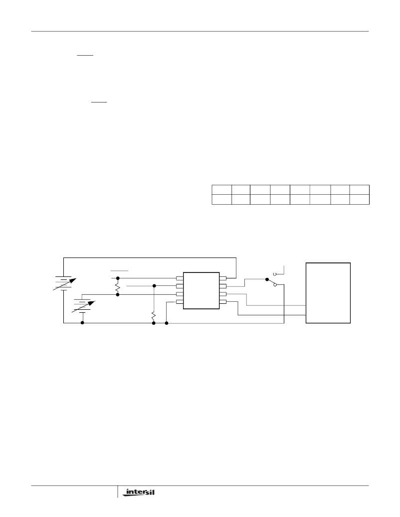
�Figure� 4.� Sample� V� TRIP� Reset� Circuit�
�V� P�
�Adjust�
�V� TRIP1�
�Adj.�
�V2FAIL�
�RESET�
�1� 8�
�3� SOIC� 7�
�2� X4041x� 6�
�4�
�5�
�Run�
�SCL�
�μC�
�V� TRIP2�
�Adj.�
�5�
�4.7K�
�SDA�
�FN8116.0�
�March� 28,� 2005�
�相关PDF资料 |
PDF描述 |
|---|---|
| RCC43DRYH-S93 | CONN EDGECARD 86POS DIP .100 SLD |
| X40410V8-AT1 | IC VOLTAGE MON DUAL W/SUP 8TSSOP |
| FMC07DREF | CONN EDGECARD 14POS .100 EYELET |
| X40410V8-A | IC VOLTAGE MON DUAL W/SUP 8TSSOP |
| X40410S8I-CT1 | IC VOLTAGE MON DUAL W/SUP 8-SOIC |
相关代理商/技术参数 |
参数描述 |
|---|---|
| X40410V8-BT1 | 功能描述:IC VOLTAGE MON DUAL W/SUP 8TSSOP RoHS:否 类别:集成电路 (IC) >> PMIC - 监控器 系列:- 标准包装:100 系列:- 类型:简单复位/加电复位 监视电压数目:1 输出:- 复位:低有效 复位超时:最小为 100 ms 电压 - 阀值:4.38V 工作温度:0°C ~ 70°C 安装类型:表面贴装 封装/外壳:8-TSSOP(0.173",4.40mm 宽) 供应商设备封装:8-TSSOP 包装:管件 |
| X40410V8-C | 功能描述:IC VOLTAGE MON DUAL W/SUP 8TSSOP RoHS:否 类别:集成电路 (IC) >> PMIC - 监控器 系列:- 标准包装:100 系列:- 类型:简单复位/加电复位 监视电压数目:1 输出:- 复位:低有效 复位超时:最小为 100 ms 电压 - 阀值:4.38V 工作温度:0°C ~ 70°C 安装类型:表面贴装 封装/外壳:8-TSSOP(0.173",4.40mm 宽) 供应商设备封装:8-TSSOP 包装:管件 |
| X40410V8-CT1 | 功能描述:IC VOLTAGE MON DUAL W/SUP 8TSSOP RoHS:否 类别:集成电路 (IC) >> PMIC - 监控器 系列:- 标准包装:100 系列:- 类型:简单复位/加电复位 监视电压数目:1 输出:- 复位:低有效 复位超时:最小为 100 ms 电压 - 阀值:4.38V 工作温度:0°C ~ 70°C 安装类型:表面贴装 封装/外壳:8-TSSOP(0.173",4.40mm 宽) 供应商设备封装:8-TSSOP 包装:管件 |
| X40410V8I-A | 功能描述:IC VOLTAGE MON DUAL W/SUP 8TSSOP RoHS:否 类别:集成电路 (IC) >> PMIC - 监控器 系列:- 标准包装:100 系列:- 类型:简单复位/加电复位 监视电压数目:1 输出:- 复位:低有效 复位超时:最小为 100 ms 电压 - 阀值:4.38V 工作温度:0°C ~ 70°C 安装类型:表面贴装 封装/外壳:8-TSSOP(0.173",4.40mm 宽) 供应商设备封装:8-TSSOP 包装:管件 |
| X40410V8I-AT1 | 功能描述:IC VOLTAGE MON DUAL W/SUP 8TSSOP RoHS:否 类别:集成电路 (IC) >> PMIC - 监控器 系列:- 标准包装:100 系列:- 类型:简单复位/加电复位 监视电压数目:1 输出:- 复位:低有效 复位超时:最小为 100 ms 电压 - 阀值:4.38V 工作温度:0°C ~ 70°C 安装类型:表面贴装 封装/外壳:8-TSSOP(0.173",4.40mm 宽) 供应商设备封装:8-TSSOP 包装:管件 |
发布紧急采购,3分钟左右您将得到回复。