- 您现在的位置:买卖IC网 > PDF目录13101 > X4043P-2.7 (Intersil)IC CPU SUPERV 4K EE RST LO 8DIP PDF资料下载
参数资料
| 型号: | X4043P-2.7 |
| 厂商: | Intersil |
| 文件页数: | 11/24页 |
| 文件大小: | 0K |
| 描述: | IC CPU SUPERV 4K EE RST LO 8DIP |
| 标准包装: | 50 |
| 类型: | 简单复位/加电复位 |
| 监视电压数目: | 1 |
| 输出: | 开路漏极或开路集电极 |
| 复位: | 低有效 |
| 复位超时: | 最小为 100 ms |
| 电压 - 阀值: | 2.62V |
| 工作温度: | 0°C ~ 70°C |
| 安装类型: | 通孔 |
| 封装/外壳: | 8-DIP(0.300",7.62mm) |
| 供应商设备封装: | 8-PDIP |
| 包装: | 管件 |
�� �
�
�X4043,� X4045�
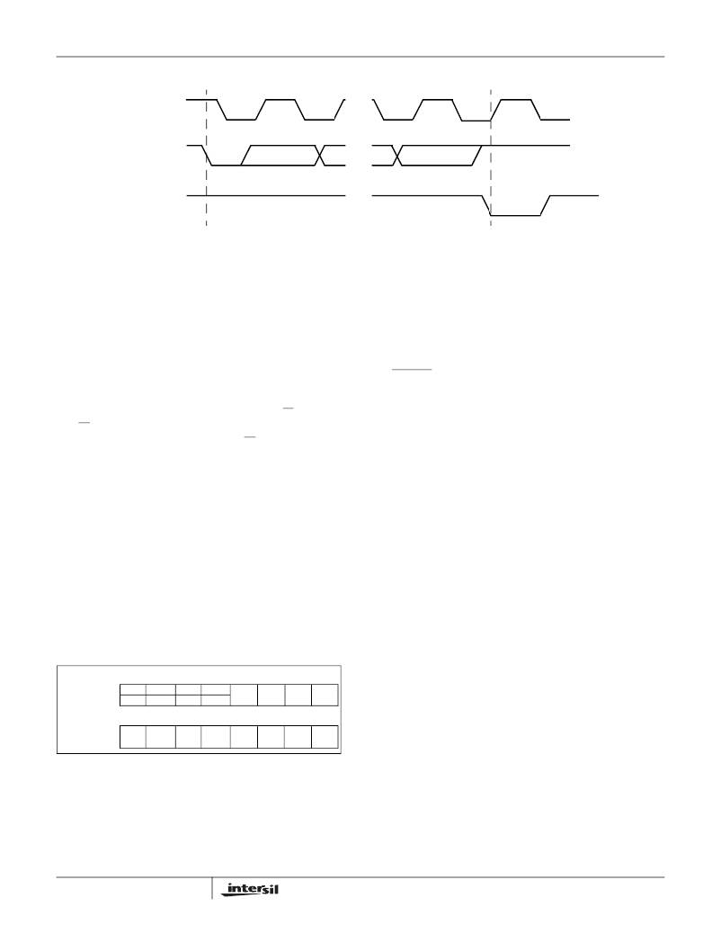
�Figure� 8.� Acknowledge� Response� From� Receiver�
�SCL� from�
�Master�
�1�
�8�
�9�
�Data� Output�
�from�
�Transmitter�
�Data� Output�
�from� Receiver�
�Start�
�X4043/45� ADDRESSING�
�Slave� Address� Byte�
�Following� a� start� condition,� the� master� must� output� a�
�slave� address� byte.� This� byte� consists� of� several� parts:�
�–� a� device� type� identifier� that� is� ‘1010’� to� access� the�
�array� and� ‘1011’� to� access� the� control� register.�
�–� two� bits� of� ‘0’.�
�–� one� bit� that� becomes� the� MSB� of� the� address.�
�–� one� bit� of� the� slave� command� byte� is� a� R/W� bit.� The�
�R/W� bit� of� the� slave� address� byte� defines� the� opera-�
�tion� to� be� performed.� When� the� R/W� bit� is� a� one,�
�then� a� read� operation� is� selected.� A� zero� selects� a�
�write� operation.� Refer� to� Figure� 8.�
�–� After� loading� the� entire� slave� address� byte� from� the�
�SDA� bus,� the� device� compares� the� input� slave� byte�
�data� to� the� proper� slave� byte.� Upon� a� correct� compare,�
�the� device� outputs� an� acknowledge� on� the� SDA� line.�
�Word� Address�
�The� word� address� is� either� supplied� by� the� master� or�
�obtained� from� an� internal� counter.� The� internal� counter�
�is� undefined� on� a� power-up� condition.�
�Slave� Address� Byte�
�Figure� 9.� X4043/45� Addressing�
�Slave� Byte�
�Acknowledge�
�Operational� Notes�
�The� device� powers-up� in� the� following� state:�
�–� The� device� is� in� the� low� power� standby� state.�
�–� The� WEL� bit� is� set� to� ‘0’.� In� this� state� it� is� not� possi-�
�ble� to� write� to� the� device.�
�–� SDA� pin� is� the� input� mode.�
�–� RESET� signal� is� active� for� t� PURST� .�
�SERIAL� WRITE� OPERATIONS�
�Byte� Write�
�For� a� write� operation,� the� device� requires� the� slave�
�address� byte� and� a� word� address� byte.� This� gives� the�
�master� access� to� any� one� of� the� words� in� the� array.�
�After� receipt� of� the� word� address� byte,� the� device�
�responds� with� an� acknowledge,� and� awaits� the� next�
�eight� bits� of� data.� After� receiving� the� 8� bits� of� the� data�
�byte,� the� device� again� responds� with� an� acknowledge.�
�The� master� then� terminates� the� transfer� by� generating� a�
�stop� condition,� at� which� time� the� device� begins� the� inter-�
�nal� write� cycle� to� the� nonvolatile� memory.� During� this�
�internal� write� cycle,� the� device� inputs� are� disabled,� so� the�
�device� will� not� respond� to� any� requests� from� the� master.�
�The� SDA� output� is� at� high� impedance.� See� Figure� 10.�
�A� write� to� a� protected� block� of� memory� will� suppress�
�the� acknowledge� bit.�
�Array�
�Control� Reg.�
�1�
�1�
�0�
�0�
�1�
�1�
�0�
�1�
�0�
�0�
�A8�
�R/W�
�Word� Address�
�A7�
�A6�
�A5�
�A4�
�A3�
�A2�
�A1�
�A0�
�11�
�FN8118.2�
�March� 16,� 2006�
�相关PDF资料 |
PDF描述 |
|---|---|
| C0603C0G1E150J | CAP CER 15PF 25V 5% NP0 0201 |
| 420MXH120MEFCSN22X25 | CAP ALUM 120UF 420V 20% SNAP-IN |
| VE-J7J-CZ-B1 | CONVERTER MOD DC/DC 36V 25W |
| GMM15DTMN-S273 | CONN EDGECARD 30POS R/A .156 SLD |
| 50MXC4700MEFCSN25X35 | CAP ALUM 4700UF 50V 20% SNAP-IN |
相关代理商/技术参数 |
参数描述 |
|---|---|
| X4043P-4.5A | 功能描述:IC SUPERVISOR CPU 4K EE 8-DIP RoHS:否 类别:集成电路 (IC) >> PMIC - 监控器 系列:- 标准包装:100 系列:- 类型:简单复位/加电复位 监视电压数目:1 输出:- 复位:低有效 复位超时:最小为 100 ms 电压 - 阀值:4.38V 工作温度:0°C ~ 70°C 安装类型:表面贴装 封装/外壳:8-TSSOP(0.173",4.40mm 宽) 供应商设备封装:8-TSSOP 包装:管件 |
| X4043P8 | 制造商:未知厂家 制造商全称:未知厂家 功能描述:Analog IC |
| X4043P8-2.7 | 制造商:未知厂家 制造商全称:未知厂家 功能描述:Analog IC |
| X4043P8-2.7A | 制造商:未知厂家 制造商全称:未知厂家 功能描述:Analog IC |
| X4043P8-4.5A | 制造商:未知厂家 制造商全称:未知厂家 功能描述:Analog IC |
发布紧急采购,3分钟左右您将得到回复。