参数资料
| 型号: | X9252WV24IZ-2.7 |
| 厂商: | Intersil |
| 文件页数: | 4/20页 |
| 文件大小: | 0K |
| 描述: | IC POT DGTL QUAD 24-TSSOP |
| 标准包装: | 62 |
| 系列: | XDCP™ |
| 接片: | 256 |
| 电阻(欧姆): | 10k |
| 电路数: | 4 |
| 温度系数: | 标准值 ±300 ppm/°C |
| 存储器类型: | 非易失 |
| 接口: | I²C(芯片选择,设备位址,增/减) |
| 电源电压: | 2.7 V ~ 5.5 V |
| 工作温度: | -40°C ~ 85°C |
| 安装类型: | 表面贴装 |
| 封装/外壳: | 24-TSSOP(0.173",4.40mm 宽) |
| 供应商设备封装: | 24-TSSOP |
| 包装: | 管件 |
| 产品目录页面: | 1237 (CN2011-ZH PDF) |
12
FN8167.2
November 14, 2005
To read or write the contents of a single Data Register or Wiper Register:
1.
Load the status register (using a write command) to select the row (See Figure 6)
Writing a 1, 3, 5, or 7 to the Status Register specifies that the subsequent read or write command will access a Data Register. This Status
Register operation also initiates a transfer of the contents of the selected data register to its associated WCR for all DCPs. So, for example,
writing ‘03h’ to the status register causes the value in DR01 to move to WCR0, DR11 to move to WCR1, DR21 to move to WCR2, and DR31
to move to WCR3.
Writing a 0 to bit ‘0’ of the Status Register specifies that the subsequent read or write command will access a Wiper Counter Register. Each
WCR can be written to individually, without affecting the contents of any other.
2.
Access the desired DR or WCR using a new write or read command (see Figure 7 for write and Figure 9 for read.)
Specify the desired column (DCP number) by sending the DCP address as part of this read or write command.
TABLE 2. REGISTER NUMBERING
STATUS REG (Note 1) (Addr: 07H)
REGISTERED SELECTED (Note 2)
RESERVED
BITS 7-3
DRSel1
bit 2
DRSel0
bit 1
NVEnable
bit 0
DCP0
DCP1
DCP2
DCP3
(Addr: 00h)
(Addr: 01h)
(Addr: 02h)
(Addr: 03h)
Reserved
X
0
WCR0
WCR1
WCR2
WCR3
0
1
DR00
DR10
DR20
DR30
0
1
DR01
DR11
DR21
DR31
1
0
1
DR02
DR12
DR22
DR32
1
DR03
DR13
DR23
DR33
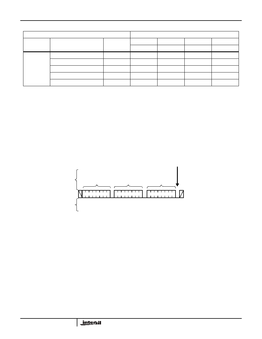
S
t
a
r
t
S
t
o
p
Slave
Address
Status Register
Address
Data
A
C
K
A
C
K
Signal at SDA
Signals from
the Slave
Signals from
the Master
0
A
C
K
If bit 0 of data byte = 1,
DR contents move to WCR
during this ACK period
01 0 1
0 0 0 0 0 1 1 1
0 0 0 0 0 x x 1
DR select
FIGURE 6. STATUS REGISTER WRITE (USES STANDARD BYTE WRITE SEQUENCE TO SET UP ACCESS TO A DATA REGISTER)
X9252
相关PDF资料 |
PDF描述 |
|---|---|
| VE-B30-MW-B1 | CONVERTER MOD DC/DC 5V 100W |
| X9252YV24IZ-2.7 | IC POT DGTL QUAD 24-TSSOP |
| VE-B30-MV | CONVERTER MOD DC/DC 5V 150W |
| VE-J5K-MZ | CONVERTER MOD DC/DC 40V 25W |
| VI-J2Y-MZ | CONVERTER MOD DC/DC 3.3V 16.5W |
相关代理商/技术参数 |
参数描述 |
|---|---|
| X9252YV24-2.7 | 功能描述:IC DCP QUAD 2.8K 256TAP 24-TSSOP RoHS:否 类别:集成电路 (IC) >> 数据采集 - 数字电位器 系列:XDCP™ 标准包装:2,500 系列:XDCP™ 接片:256 电阻(欧姆):100k 电路数:1 温度系数:标准值 ±300 ppm/°C 存储器类型:非易失 接口:I²C(设备位址) 电源电压:2.7 V ~ 5.5 V 工作温度:0°C ~ 70°C 安装类型:表面贴装 封装/外壳:14-TSSOP(0.173",4.40mm 宽) 供应商设备封装:14-TSSOP 包装:带卷 (TR) |
| X9252YV24I-2.7 | 功能描述:IC DCP QUAD 2.8K 256TAP 24-TSSOP RoHS:否 类别:集成电路 (IC) >> 数据采集 - 数字电位器 系列:XDCP™ 标准包装:2,500 系列:XDCP™ 接片:256 电阻(欧姆):100k 电路数:1 温度系数:标准值 ±300 ppm/°C 存储器类型:非易失 接口:I²C(设备位址) 电源电压:2.7 V ~ 5.5 V 工作温度:0°C ~ 70°C 安装类型:表面贴装 封装/外壳:14-TSSOP(0.173",4.40mm 宽) 供应商设备封装:14-TSSOP 包装:带卷 (TR) |
| X9252YV24IZ-2.7 | 功能描述:IC POT DGTL QUAD 24-TSSOP RoHS:是 类别:集成电路 (IC) >> 数据采集 - 数字电位器 系列:XDCP™ 产品培训模块:Lead (SnPb) Finish for COTS Obsolescence Mitigation Program 标准包装:1 系列:- 接片:256 电阻(欧姆):100k 电路数:1 温度系数:标准值 35 ppm/°C 存储器类型:非易失 接口:3 线串口 电源电压:2.7 V ~ 5.25 V 工作温度:-40°C ~ 85°C 安装类型:表面贴装 封装/外壳:8-WDFN 裸露焊盘 供应商设备封装:8-TDFN-EP(3x3) 包装:剪切带 (CT) 产品目录页面:1399 (CN2011-ZH PDF) 其它名称:MAX5423ETA+TCT |
| X9258 | 制造商:INTERSIL 制造商全称:Intersil Corporation 功能描述:Low Noise/Low Power/2-Wire Bus/256 Taps |
| X9258)06 | 制造商:INTERSIL 制造商全称:Intersil Corporation 功能描述:Quad Digital Controlled Potentiometers |
发布紧急采购,3分钟左右您将得到回复。