参数资料
| 型号: | X9252WV24IZ-2.7 |
| 厂商: | Intersil |
| 文件页数: | 6/20页 |
| 文件大小: | 0K |
| 描述: | IC POT DGTL QUAD 24-TSSOP |
| 标准包装: | 62 |
| 系列: | XDCP™ |
| 接片: | 256 |
| 电阻(欧姆): | 10k |
| 电路数: | 4 |
| 温度系数: | 标准值 ±300 ppm/°C |
| 存储器类型: | 非易失 |
| 接口: | I²C(芯片选择,设备位址,增/减) |
| 电源电压: | 2.7 V ~ 5.5 V |
| 工作温度: | -40°C ~ 85°C |
| 安装类型: | 表面贴装 |
| 封装/外壳: | 24-TSSOP(0.173",4.40mm 宽) |
| 供应商设备封装: | 24-TSSOP |
| 包装: | 管件 |
| 产品目录页面: | 1237 (CN2011-ZH PDF) |
14
FN8167.2
November 14, 2005
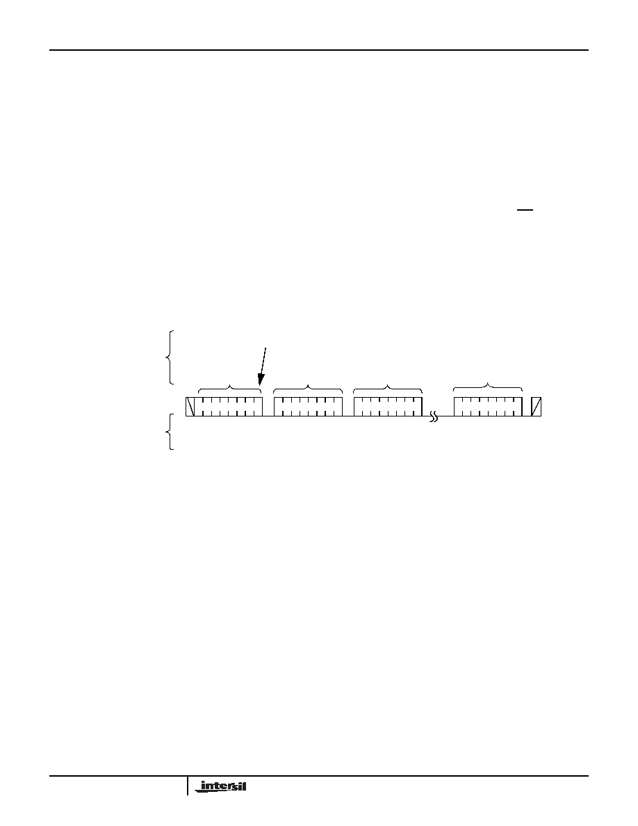
Page Write Operation
As stated previously, the memory is organized as a single
Status Register (SR), and four pages of four registers each.
Each page contains one Data Register for each DCP. The
order of the bytes within a page is DR0i, followed by DR1i,
followed by DR2i, and then DR3i, with i being the Data
Register number (0, 1, 2, or 3). Normally a page write
operation will be used to efficiently update all four data
registers and WCR in a single write command, starting at
DCP0 and finishing with DCP3.
In order to perform a Page Write operation to the memory
array, the NVEnable bit in the SR must first be set to “1”.
A Page Write operation is initiated in the same manner as
the byte write operation; but instead of terminating the write
cycle after the first data byte is transferred, the master can
transmit up to 4 bytes (See Figure 8). After the receipt of
each byte, the X9252 responds with an ACK, and the
internal DCP address counter is incremented by one. The
page address remains constant. When the counter reaches
the end of the page (DR3i, 03hex), it “rolls over” and goes
back to the first byte of the same page (DR0i, 00hex).
For example, if the master writes 3 bytes to a page starting
at location DR22, the first 2 bytes are written to locations
DR22 and DR32, while the last byte is written to locations
DR02. Afterwards, the DCP counter would point to location
DR12. If the master supplies more than 4 bytes of data, then
new data overwrites the previous data, one byte at a time.
The master terminates the loading of Data Bytes by issuing
a STOP condition, which initiates the nonvolatile write cycle.
As with the Byte Write operation, all inputs are disabled until
completion of the internal write cycle. If the WP pin is low,
the nonvolatile write cycle doesn’t start and the bytes are
discarded.
Notice that the Data Bytes are also written to the WCR of the
corresponding DCPs, therefore in the above example,
WCR2, WCR3, and WCR0 are also written and WCR1 is
updated with the contents of DR12.
2 < n < 4
Signals from the
Master
Signals from the
Slave
Signal at SDA
S
t
a
r
t
Slave
Address
Byte
A
C
K
A
C
K
0
11
Data Byte (1)
S
t
o
p
A
C
K
A
C
K
Data Byte (n)
Write
FIGURE 8. PAGE WRITE OPERATION
X9252
相关PDF资料 |
PDF描述 |
|---|---|
| VE-B30-MW-B1 | CONVERTER MOD DC/DC 5V 100W |
| X9252YV24IZ-2.7 | IC POT DGTL QUAD 24-TSSOP |
| VE-B30-MV | CONVERTER MOD DC/DC 5V 150W |
| VE-J5K-MZ | CONVERTER MOD DC/DC 40V 25W |
| VI-J2Y-MZ | CONVERTER MOD DC/DC 3.3V 16.5W |
相关代理商/技术参数 |
参数描述 |
|---|---|
| X9252YV24-2.7 | 功能描述:IC DCP QUAD 2.8K 256TAP 24-TSSOP RoHS:否 类别:集成电路 (IC) >> 数据采集 - 数字电位器 系列:XDCP™ 标准包装:2,500 系列:XDCP™ 接片:256 电阻(欧姆):100k 电路数:1 温度系数:标准值 ±300 ppm/°C 存储器类型:非易失 接口:I²C(设备位址) 电源电压:2.7 V ~ 5.5 V 工作温度:0°C ~ 70°C 安装类型:表面贴装 封装/外壳:14-TSSOP(0.173",4.40mm 宽) 供应商设备封装:14-TSSOP 包装:带卷 (TR) |
| X9252YV24I-2.7 | 功能描述:IC DCP QUAD 2.8K 256TAP 24-TSSOP RoHS:否 类别:集成电路 (IC) >> 数据采集 - 数字电位器 系列:XDCP™ 标准包装:2,500 系列:XDCP™ 接片:256 电阻(欧姆):100k 电路数:1 温度系数:标准值 ±300 ppm/°C 存储器类型:非易失 接口:I²C(设备位址) 电源电压:2.7 V ~ 5.5 V 工作温度:0°C ~ 70°C 安装类型:表面贴装 封装/外壳:14-TSSOP(0.173",4.40mm 宽) 供应商设备封装:14-TSSOP 包装:带卷 (TR) |
| X9252YV24IZ-2.7 | 功能描述:IC POT DGTL QUAD 24-TSSOP RoHS:是 类别:集成电路 (IC) >> 数据采集 - 数字电位器 系列:XDCP™ 产品培训模块:Lead (SnPb) Finish for COTS Obsolescence Mitigation Program 标准包装:1 系列:- 接片:256 电阻(欧姆):100k 电路数:1 温度系数:标准值 35 ppm/°C 存储器类型:非易失 接口:3 线串口 电源电压:2.7 V ~ 5.25 V 工作温度:-40°C ~ 85°C 安装类型:表面贴装 封装/外壳:8-WDFN 裸露焊盘 供应商设备封装:8-TDFN-EP(3x3) 包装:剪切带 (CT) 产品目录页面:1399 (CN2011-ZH PDF) 其它名称:MAX5423ETA+TCT |
| X9258 | 制造商:INTERSIL 制造商全称:Intersil Corporation 功能描述:Low Noise/Low Power/2-Wire Bus/256 Taps |
| X9258)06 | 制造商:INTERSIL 制造商全称:Intersil Corporation 功能描述:Quad Digital Controlled Potentiometers |
发布紧急采购,3分钟左右您将得到回复。