参数资料
| 型号: | X9401WV24Z-2.7 |
| 厂商: | Intersil |
| 文件页数: | 13/18页 |
| 文件大小: | 0K |
| 描述: | IC XDCP QUAD 64-TAP 10K 24-TSSOP |
| 标准包装: | 62 |
| 系列: | XDCP™ |
| 接片: | 64 |
| 电阻(欧姆): | 10k |
| 电路数: | 4 |
| 温度系数: | 标准值 ±300 ppm/°C |
| 存储器类型: | 非易失 |
| 接口: | 6 线 SPI(芯片选择,设备位址) |
| 电源电压: | 2.7 V ~ 5.5 V |
| 工作温度: | 0°C ~ 70°C |
| 安装类型: | 表面贴装 |
| 封装/外壳: | 24-TSSOP(0.173",4.40mm 宽) |
| 供应商设备封装: | 24-TSSOP |
| 包装: | 管件 |
4
FN8190.4
October 13, 2009
Data Registers
Each potentiometer has four 6-bit nonvolatile data registers.
These can be read or written directly by the host. Data can
also be transferred between any of the four data registers
and the associated Wiper Counter Register. All operations
changing data in one of the data registers is a nonvolatile
operation and will take a maximum of 10ms.
If the application does not require storage of multiple
settings for the potentiometer, the data registers can be used
as memory locations for system parameters or user
preference data.
DATA REGISTER DETAIL
Write in Process
The contents of the Data Registers are saved to nonvolatile
memory when the CS pin goes from LOW to HIGH after a
complete write sequence is received by the device. The
progress of this internal write operation can be monitored by
a Write In Process bit (WIP). The WIP bit is read with a Read
Status command.
Instructions
Identification (ID) Byte
The first byte sent to the X9401 from the host, following a CS
going HIGH to LOW, is called the Identification byte. The
most significant four bits of the slave address are a device
type identifier. For the X9401 this is fixed as 0101[B] (refer to
The two least significant bits in the ID byte select one of four
devices on the bus. The physical device address is defined
by the state of the A0 - A1 input pins. The X9401 compares
the serial data stream with the address input state; a
successful compare of both address bits is required for the
X9401 to successfully continue the command sequence.
The A0 - A1 inputs can be actively driven by CMOS input
signals or tied to VCC or VSS. The remaining two bits in the
slave byte must be set to 0.
Instruction Byte
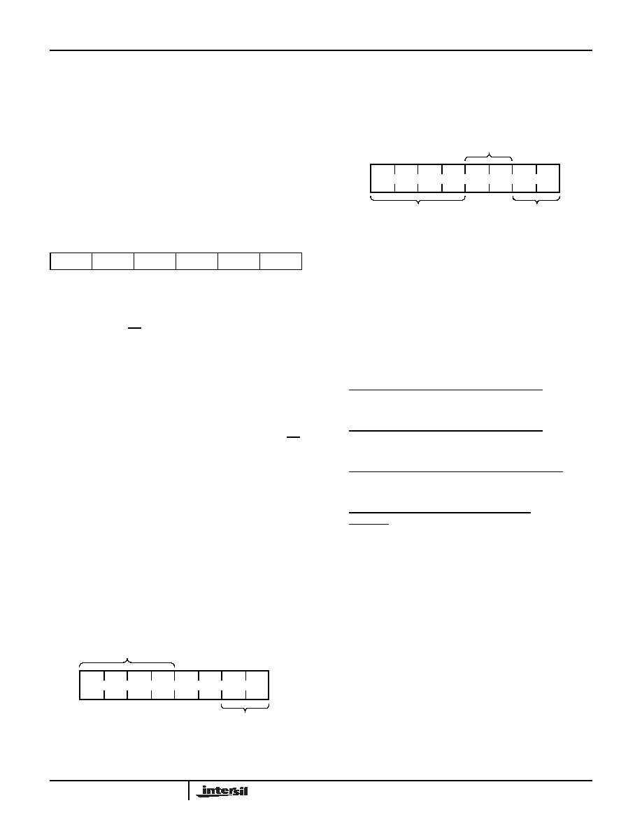
The next byte sent to the X9401 contains the instruction and
register pointer information. The four most significant bits are
the instruction. The next four bits point to one of the four pots
and, when applicable, they point to one of four associated
registers. The format is shown below in Figure 2.
I
The four high order bits of the instruction byte specify the
operation. The next two bits (R1 and R0) select one of the
four registers that is to be acted upon when a register
oriented instruction is issued. The last two bits (P1 and P0)
selects which one of the four potentiometers is to be affected
by the instruction.
Four of the ten instructions are two bytes in length and end
with the transmission of the instruction byte. These
instructions are:
XFR Data Register to Wiper Counter Register: This
transfers the contents of one specified Data Register to
the associated Wiper Counter Register.
XFR Wiper Counter Register to Data Register: This
transfers the contents of the specified Wiper Counter
Register to the specified associated Data Register.
Global XFR Data Register to Wiper Counter Register: This
transfers the contents of all specified Data Registers to the
associated Wiper Counter Registers.
Global XFR Wiper Counter Register to Data
Register: This transfers the contents of all Wiper Counter
Registers to the specified associated Data Registers.
The basic sequence of the two byte instructions is illustrated
in Figure 3. These two-byte instructions exchange data
between the WCR and one of the data registers. A transfer
from a data register to a WCR is essentially a write to a static
RAM, with the static RAM controlling the wiper position. The
response of the wiper to this action will be delayed by tWRL.
A transfer from the WCR (current wiper position), to a data
register is a write to nonvolatile memory and takes a
minimum of tWR to complete. The transfer can occur
between one of the four potentiometers and one of its
associated registers; or it may occur globally, where the
transfer occurs between all potentiometers and one
associated register.
Five instructions require a three-byte sequence to complete.
These instructions transfer data between the host and the
X9401; either between the host and one of the data registers
(MSB)
(LSB)
D5
D4
D3
D2
D1
D0
NV
1
00
A1
A0
DEVICE TYPE
IDENTIFIER
DEVICE ADDRESS
1
FIGURE 1. IDENTIFICATION BYTE FORMAT
I1
I2
I3
I0
R1
R0
P1
P0
POT SELECT
INSTRUCTIONS
FIGURE 2. IDENTIFICATION BYTE FORMAT
X9401
相关PDF资料 |
PDF描述 |
|---|---|
| MS3450W22-6SY | CONN RCPT 3POS WALL MNT W/SCKT |
| IDT72V70810PFG8 | IC DGTL SW 1024X1024 3.3V 64TQFP |
| IDT72V70810PF8 | IC DGTL SW 1024X1024 3.3V 64TQFP |
| MS3450W22-6SX | CONN RCPT 3POS WALL MNT W/SCKT |
| IDT72V70810TFG8 | IC DGTL SW 1024X1024 64-STQFP |
相关代理商/技术参数 |
参数描述 |
|---|---|
| X9401WV24ZT1 | 功能描述:IC XDCP QUAD 64-TAP 10K 24-TSSOP RoHS:是 类别:集成电路 (IC) >> 数据采集 - 数字电位器 系列:XDCP™ 产品培训模块:Lead (SnPb) Finish for COTS Obsolescence Mitigation Program 标准包装:2,500 系列:- 接片:256 电阻(欧姆):100k 电路数:2 温度系数:标准值 35 ppm/°C 存储器类型:易失 接口:6 线串行(芯片选择,递增,增/减) 电源电压:2.6 V ~ 5.5 V 工作温度:-40°C ~ 125°C 安装类型:表面贴装 封装/外壳:14-TSSOP(0.173",4.40mm 宽) 供应商设备封装:14-TSSOP 包装:带卷 (TR) |
| X9401YS24I-2.7 | 功能描述:IC XDCP QUAD 64-TAP 2.5K 24-SOIC RoHS:否 类别:集成电路 (IC) >> 数据采集 - 数字电位器 系列:XDCP™ 产品培训模块:Lead (SnPb) Finish for COTS Obsolescence Mitigation Program 标准包装:2,500 系列:- 接片:32 电阻(欧姆):50k 电路数:1 温度系数:标准值 50 ppm/°C 存储器类型:易失 接口:3 线串行(芯片选择,递增,增/减) 电源电压:2.7 V ~ 5.5 V 工作温度:-40°C ~ 85°C 安装类型:表面贴装 封装/外壳:SOT-23-6 细型,TSOT-23-6 供应商设备封装:TSOT-23-6 包装:带卷 (TR) |
| X9401YV24I-2.7 | 功能描述:IC XDCP QUAD 64-TAP 2.5K 24TSSOP RoHS:否 类别:集成电路 (IC) >> 数据采集 - 数字电位器 系列:XDCP™ 产品培训模块:Lead (SnPb) Finish for COTS Obsolescence Mitigation Program 标准包装:2,500 系列:- 接片:32 电阻(欧姆):50k 电路数:1 温度系数:标准值 50 ppm/°C 存储器类型:易失 接口:3 线串行(芯片选择,递增,增/减) 电源电压:2.7 V ~ 5.5 V 工作温度:-40°C ~ 85°C 安装类型:表面贴装 封装/外壳:SOT-23-6 细型,TSOT-23-6 供应商设备封装:TSOT-23-6 包装:带卷 (TR) |
| X9408 | 制造商:INTERSIL 制造商全称:Intersil Corporation 功能描述:Quad Digitally Controlled (XDCP?) Potentiometers |
| X9408_09 | 制造商:INTERSIL 制造商全称:Intersil Corporation 功能描述:Quad Digitally Controlled (XDCP?) Potentiometers |
发布紧急采购,3分钟左右您将得到回复。