参数资料
| 型号: | X9420WP16Z |
| 厂商: | Intersil |
| 文件页数: | 4/19页 |
| 文件大小: | 0K |
| 描述: | IC DGTL POT 1CH 16PDIP |
| 标准包装: | 30 |
| 系列: | XDCP™ |
| 接片: | 64 |
| 电阻(欧姆): | 10k |
| 电路数: | 1 |
| 温度系数: | 标准值 ±300 ppm/°C |
| 存储器类型: | 非易失 |
| 接口: | 5 线 SPI(芯片选择,设备位址) |
| 电源电压: | 4.5 V ~ 5.5 V |
| 工作温度: | 0°C ~ 70°C |
| 安装类型: | 通孔 |
| 封装/外壳: | 16-DIP(0.300",7.62mm) |
| 供应商设备封装: | 16-DIP |
| 包装: | 管件 |
12
FN8195.1
April 26, 2006
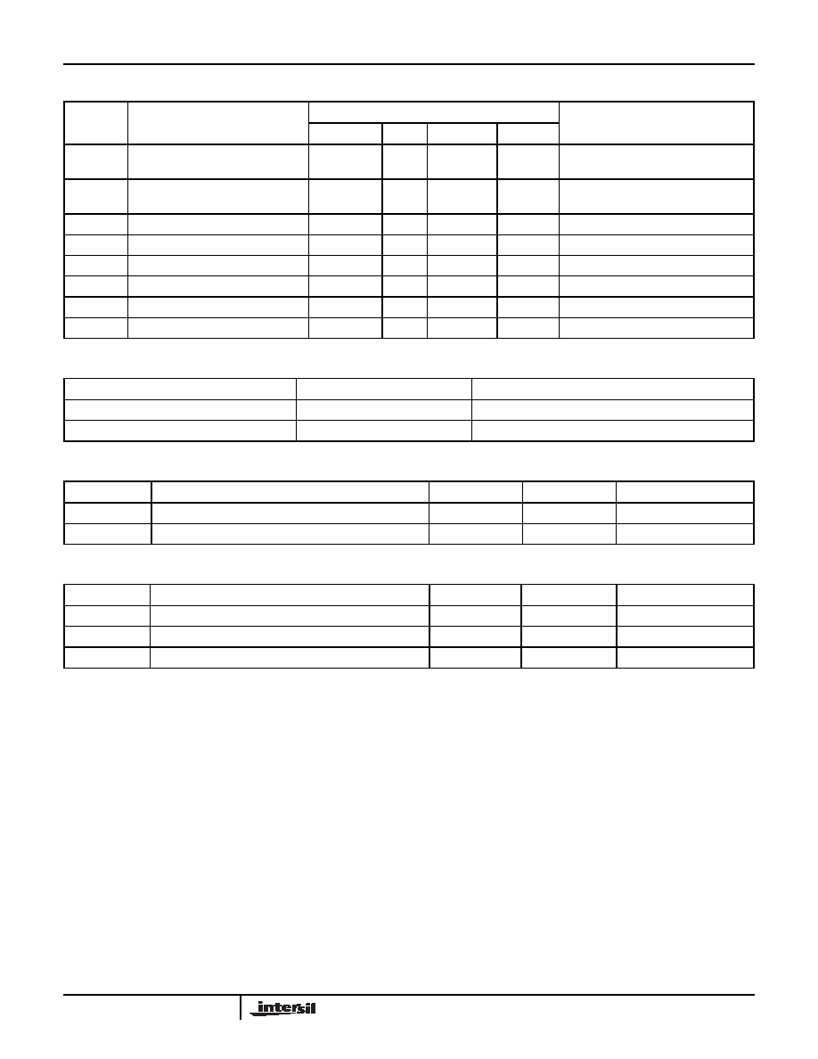
D.C. OPERATING CHARACTERISTICS (Over the recommended operating conditions unless otherwise specified.)
ENDURANCE AND DATA RETENTION
CAPACITANCE
POWER-UP TIMING
POWER-UP REQUIREMENTS (Power-up sequencing can affect correct recall of the wiper registers)
The preferred power-on sequence is as follows: First VCC, then V+ and V-, and then the potentiometer pins, RH, RL,
and RW. Voltage should not be applied to the potentiometer pins before V+ or V- is applied. The VCC ramp rate
specification should be met, and any glitches or slope changes in the VCC line should be held to <100mV if possible.
If VCC powers down, it should be held below 0.1V for more than 1 second before powering up again in order for
proper wiper register recall. Also, VCC should not reverse polarity by more than 0.5V. Recall of wiper position will not
be complete until VCC, V+ and V- reach their final value.
Notes: (5) This parameter is periodically sampled and not 100% tested.
(6) tPUR and tPUW are the delays required from the time the third (last) power supply (VCC, V+ or V-) is stable until the specific instruction
can be issued. These parameters are periodically sampled and not 100% tested.
Symbol
Parameter
Limits
Test Conditions
Min.
Typ.
Max.
Units
ICC1
VCC Supply Current (Active)
400
A
fSCK = 2MHz, SO = Open,
Other Inputs = VSS
ICC2
VCC Supply Current
(Non-volatile Write)
1mA
fSCK = 2MHz, SO = Open,
Other Inputs = VSS
ISB
VCC Current (Standby)
1
μA
SCK = SI = VSS, Addr. = VSS
ILI
Input Leakage Current
10
μAVIN = VSS to VCC
ILO
Output Leakage Current
10
μAVOUT = VSS to VCC
VIH
Input HIGH Voltage
VCC x 0.7
VCC + 0.5
V
VIL
Input LOW Voltage
-0.5
VCC x 0.1
V
VOL
Output LOW Voltage
0.4
V
IOL = 3mA
Parameter
Min.
Units
Minimum Endurance
100,000
Data Changes per Bit per Register
Data Retention
100
Years
Symbol
Test
Max.
Units
Test Conditions
COUT(5)
Output Capacitance (SO)
8
pF
VOUT = 0V
CIN(5)
Input Capacitance (A0, SI, and SCK)
6
pF
VIN = 0V
Symbol
Parameter
Max.
Units
tPUR(6)
Power-up to Initiation of Read Operation
1
ms
tPUW(6)
Power-up to Initiation of Write Operation
5
ms
tRVCC
VCC Power-up Ramp
0.2
50
V/msec
X9420
相关PDF资料 |
PDF描述 |
|---|---|
| MS3108A28-18S | CONN PLUG 12POS RT ANG W/SCKT |
| MS27472E18B96P | CONN RCPT 9POS WALL MT W/PINS |
| VE-J1F-MZ-S | CONVERTER MOD DC/DC 72V 25W |
| MS3108E28-10P | CONN PLUG 7POS RT ANG W/PINS |
| MS27468E25F35PB | CONN RCPT 128POS JAM NUT W/PINS |
相关代理商/技术参数 |
参数描述 |
|---|---|
| X9420WP-2.7 | 制造商:XICOR 制造商全称:Xicor Inc. 功能描述:Single Digitally Controlled (XDCP) Potentiometer |
| X9420WPI | 制造商:XICOR 制造商全称:Xicor Inc. 功能描述:Single Digitally Controlled (XDCP) Potentiometer |
| X9420WPI-2.7 | 制造商:XICOR 制造商全称:Xicor Inc. 功能描述:Single Digitally Controlled (XDCP) Potentiometer |
| X9420WPM | 制造商:XICOR 制造商全称:Xicor Inc. 功能描述:Single Digitally Controlled (XDCP) Potentiometer |
| X9420WPM-2.7 | 制造商:XICOR 制造商全称:Xicor Inc. 功能描述:Single Digitally Controlled (XDCP) Potentiometer |
发布紧急采购,3分钟左右您将得到回复。