参数资料
| 型号: | X95820WV14I-2.7T1 |
| 厂商: | Intersil |
| 文件页数: | 12/12页 |
| 文件大小: | 0K |
| 描述: | IC XDCP DUAL 256TAP 10K 14-TSSOP |
| 标准包装: | 2,500 |
| 系列: | XDCP™ |
| 接片: | 256 |
| 电阻(欧姆): | 10k |
| 电路数: | 2 |
| 温度系数: | 标准值 ±45 ppm/°C |
| 存储器类型: | 非易失 |
| 接口: | I²C(设备位址) |
| 电源电压: | 2.7 V ~ 5.5 V |
| 工作温度: | -40°C ~ 85°C |
| 安装类型: | 表面贴装 |
| 封装/外壳: | 14-TSSOP(0.173",4.40mm 宽) |
| 供应商设备封装: | 14-TSSOP |
| 包装: | 带卷 (TR) |
9
FN8212.2
July 18, 2006
Principles of Operation
The X95820 in as integrated circuit incorporating two DCPs
with their associated registers, non-volatile memory, and a
I2C serial interface providing direct communication between
a host and the potentiometers and memory.
DCP Description
Each DCP is implemented with a combination of resistor
elements and CMOS switches. The physical ends of each
DCP are equivalent to the fixed terminals of a mechanical
potentiometer (RH and RL pins). The RW pin of each DCP is
connected to intermediate nodes, and is equivalent to the
wiper terminal of a mechanical potentiometer. The position
of the wiper terminal within the DCP is controlled by an 8-bit
volatile Wiper Register (WR). Each DCP has its own WR.
When the WR of a DCP contains all zeroes (WR<7:0>: 00h),
its wiper terminal (RW) is closest to its “Low” terminal (RL).
When the WR of a DCP contains all ones (WR<7:0>: FFh),
its wiper terminal (RW) is closest to its “High” terminal (RH).
As the value of the WR increases from all zeroes (00h) to all
ones (255 decimal), the wiper moves monotonically from the
position closest to RL to the closest to RH. At the same time,
the resistance between RW and RL increases monotonically,
while the resistance between RH and RW decreases
monotonically.
While the X95820 is being powered up, all two WRs are
reset to 80h (128 decimal), which locates RW roughly at the
center between RL and RH. Soon after the power supply
voltage becomes large enough for reliable non-volatile
memory reading, the X95820 reads the value stored on two
different non-volatile Initial Value Registers (IVRs) and loads
them into their corresponding WRs.
The WRs and IVRs can be read or written directly using the
I2C serial interface as described in the following sections.
Memory Description
The X95820 contains eight non-volatile bytes. they are
accessed by I2C interface operations with Address Bytes 0
through 7 decimal. The first two non-volatile bytes at
addresses 0 and 1 contain the initial value loaded at power-
up into the volatile Wiper Registers (WRs) of DCP0 and
DCP1 respectively. Bytes at addresses 2, 3, 4, 5, and 6 are
available to the user as general purpose registers. The byte
at address 7 is reserved; the user should not write to it, and
its value should be ignored if read.
The volatile WR, and the non-volatile Initial Value Register
(IVR) of a DCP are accessed with the same Address Byte.
A volatile byte at address 8 decimal, controls what byte is
read or written when accessing DCP registers: the WR, the
IVR, or both.
When the byte at address 8 is all zeroes, which is the default
at power up:
A read operation to addresses 0 or 1 outputs the value of
the non-volatile IVRs.
A write operation to addresses 0 or 1 writes the same
value to the WR and IVR of the corresponding DCP.
When the byte at address 8 is 80h (128 decimal):
A read operation to addresses 0 or 1 outputs the value of
the volatile WR.
A write operation to addresses 0 or 1only writes to the
corresponding volatile WR.
It is not possible to write to an IVR without writing the same
value to its corresponding WR.
00h and 80h are the only values that should be written to
address 8. All other values are reserved and must not be
written to address 8.
To access the general purpose bytes at addresses 2, 3, 4, 5,
or 6, the value at address 8 must be all zeros.
The X95820 is pre-programmed with 80h in the two IVRs.
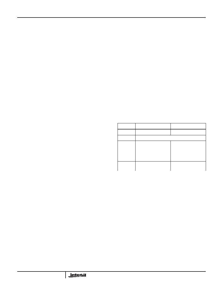
WR: Wiper Register, IVR: Initial value Register.
I2C Serial Interface
The X95820 supports a bidirectional I2C bus oriented
protocol. The protocol defines any device that sends data
onto the bus as a transmitter and the receiving device as the
receiver. The device controlling the transfer is a master and
the device being controlled is the slave. The master always
initiates data transfers and provides the clock for both
transmit and receive operations. Therefore, the X95820
operates as a slave device in all applications.
All communication over the I2C interface is conducted by
sending the MSB of each byte of data first.
Protocol Conventions
Data states on the SDA line can change only during SCL
LOW periods. SDA state changes during SCL HIGH are
reserved for indicating START and STOP conditions (See
Figure 15). On power up of the X95820 the SDA pin is in the
input mode.
TABLE 1. MEMORY MAP
ADDRESS
NON-VOLATILE
VOLATILE
8
-
Access Control
7Reserved
6
5
4
3
2
General Purpose
Not Available
1
0
IVR1
IVR0
WR1
WR0
X95820
相关PDF资料 |
PDF描述 |
|---|---|
| X95840WV20I-2.7T1 | IC XDCP QUAD 256TAP 10K 20-TSSOP |
| X96010V14IZ | IC SENSOR CONDITIONER 14-TSSOP |
| X96012V14IZT1 | IC BIAS CTRLR UNIV SNSR 14-TSSOP |
| X9C303V8T2 | IC XDCP 100-TAP 32K EE 8-TSSOP |
| X9C503ST2 | IC XDCP 100-TAP 50K EE 8-SOIC |
相关代理商/技术参数 |
参数描述 |
|---|---|
| X95820WV14IZ-2.7 | 功能描述:IC XDCP DUAL 256TAP 10K 14-TSSOP RoHS:是 类别:集成电路 (IC) >> 数据采集 - 数字电位器 系列:XDCP™ 产品培训模块:Lead (SnPb) Finish for COTS Obsolescence Mitigation Program 标准包装:2,500 系列:- 接片:256 电阻(欧姆):100k 电路数:2 温度系数:标准值 35 ppm/°C 存储器类型:易失 接口:6 线串行(芯片选择,递增,增/减) 电源电压:2.6 V ~ 5.5 V 工作温度:-40°C ~ 125°C 安装类型:表面贴装 封装/外壳:14-TSSOP(0.173",4.40mm 宽) 供应商设备封装:14-TSSOP 包装:带卷 (TR) |
| X95820WV14IZ-2.7T1 | 功能描述:IC POT DGTL DUAL 10K OHM 14TSSOP RoHS:是 类别:集成电路 (IC) >> 数据采集 - 数字电位器 系列:XDCP™ 产品培训模块:Lead (SnPb) Finish for COTS Obsolescence Mitigation Program 标准包装:1 系列:- 接片:256 电阻(欧姆):100k 电路数:1 温度系数:标准值 35 ppm/°C 存储器类型:非易失 接口:3 线串口 电源电压:2.7 V ~ 5.25 V 工作温度:-40°C ~ 85°C 安装类型:表面贴装 封装/外壳:8-WDFN 裸露焊盘 供应商设备封装:8-TDFN-EP(3x3) 包装:剪切带 (CT) 产品目录页面:1399 (CN2011-ZH PDF) 其它名称:MAX5423ETA+TCT |
| X95840 | 制造商:INTERSIL 制造商全称:Intersil Corporation 功能描述:Quad Digital Controlled Potentiometers |
| X95840_06 | 制造商:INTERSIL 制造商全称:Intersil Corporation 功能描述:Quad Digital Controlled Potentiometers |
| X95840UV20I-2.7 | 功能描述:IC XDCP QUAD 256TAP 50K 20-TSSOP RoHS:否 类别:集成电路 (IC) >> 数据采集 - 数字电位器 系列:XDCP™ 产品培训模块:Lead (SnPb) Finish for COTS Obsolescence Mitigation Program 标准包装:2,500 系列:- 接片:32 电阻(欧姆):50k 电路数:1 温度系数:标准值 50 ppm/°C 存储器类型:易失 接口:3 线串行(芯片选择,递增,增/减) 电源电压:2.7 V ~ 5.5 V 工作温度:-40°C ~ 85°C 安装类型:表面贴装 封装/外壳:SOT-23-6 细型,TSOT-23-6 供应商设备封装:TSOT-23-6 包装:带卷 (TR) |
发布紧急采购,3分钟左右您将得到回复。