参数资料
| 型号: | XC18V04PCG44C |
| 厂商: | Xilinx Inc |
| 文件页数: | 22/24页 |
| 文件大小: | 0K |
| 描述: | IC PROM REPROGR 4MB 44-PLCC |
| 标准包装: | 26 |
| 可编程类型: | 系统内可编程 |
| 存储容量: | 4Mb |
| 电源电压: | 3 V ~ 3.6 V |
| 工作温度: | 0°C ~ 70°C |
| 封装/外壳: | 44-LCC(J 形引线) |
| 供应商设备封装: | 44-PLCC(16.59x16.59) |
| 包装: | 管件 |
XC18V00 Series In-System-Programmable Configuration PROMs
DS026 (v5.2) January 11, 2008
Product Specification
7
R
IEEE 1149.1 Boundary-Scan (JTAG)
The XC18V00 family is fully compliant with the IEEE Std.
1149.1 Boundary-Scan, also known as JTAG. A Test
Access Port (TAP) and registers are provided to support all
required Boundary-Scan instructions, as well as many of
the optional instructions specified by IEEE Std. 1149.1. In
addition, the JTAG interface is used to implement in-system
programming (ISP) to facilitate configuration, erasure, and
verification operations on the XC18V00 device.
Table 4 lists the required and optional Boundary-Scan
instructions supported in the XC18V00. Refer to the IEEE Std.
1149.1 specification for a complete description of Boundary-
Scan architecture and the required and optional instructions.
Instruction Register
The Instruction Register (IR) for the XC18V00 is eight bits
wide and is connected between TDI and TDO during an
instruction scan sequence. In preparation for an instruction
scan sequence, the instruction register is parallel loaded with
a fixed instruction capture pattern. This pattern is shifted out
onto TDO (LSB first), while an instruction is shifted into the
instruction register from TDI. The detailed composition of the
instruction capture pattern is illustrated in Figure 3.
The ISP Status field, IR(4), contains logic “1” if the device is
currently in ISP mode; otherwise, it contains logic “0”. The
Security field, IR(3), contains logic “1” if the device has been
programmed with the security option turned on; otherwise, it
contains logic “0”.
X-Ref Target - Figure 3
Boundary-Scan Register
The Boundary-Scan register is used to control and observe
the
state
of
the
device
pins
during
the
EXTEST,
SAMPLE/PRELOAD, and CLAMP instructions. Each output
pin on the XC18V00 has two register stages that contribute
to the Boundary-Scan register, while each input pin only has
one register stage.
For each output pin, the register stage nearest to TDI controls
and observes the output state, and the second stage closest to
TDO controls and observes the high-Z enable state of the pin.
For each input pin, the register stage controls and observes
the input state of the pin.
Identification Registers
The IDCODE is a fixed, vendor-assigned value that is used
to electrically identify the manufacturer and type of the
device being addressed. The IDCODE register is 32 bits
wide. The IDCODE register can be shifted out for
examination by using the IDCODE instruction. The IDCODE
is available to any other system component via JTAG.
See Table 5 for the XC18V00 IDCODE values.
The IDCODE register has the following binary format:
vvvv:ffff:ffff:aaaa:aaaa:cccc:cccc:ccc1
where
v
= the die version number
f
= the family code (50h for XC18V00 family)
a
= the ISP PROM product ID (26h or 36h for the XC18V04)
c
= the company code (49h for Xilinx)
Note: The LSB of the IDCODE register is always read as logic “1”
as defined by IEEE Std. 1149.1.
Table 5 lists the IDCODE register values for XC18V00 devices.
Table 4: Boundary-Scan Instructions
Boundary-Scan
Command
Binary
Code [7:0]
Description
Required Instructions:
BYPASS
11111111
Enables BYPASS
SAMPLE/
PRELOAD
00000001
Enables Boundary-Scan
SAMPLE/PRELOAD
operation
EXTEST
00000000
Enables Boundary-Scan
EXTEST operation
Optional Instructions:
CLAMP
11111010
Enables Boundary-Scan
CLAMP operation
HIGHZ
11111100
All outputs in high-Z state
simultaneously
IDCODE
11111110
Enables shifting out
32-bit IDCODE
USERCODE
11111101
Enables shifting out
32-bit USERCODE
XC18V00 Specific Instructions:
CONFIG
11101110
Initiates FPGA configuration
by pulsing CF pin Low once
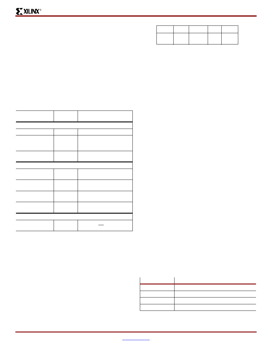
IR[7:5]
IR[4]
IR[3]
IR[2]
IR[1:0]
TDI
→
000
ISP
Status
Security
001(1)
→ TDO
Notes:
1.
IR[1:0] = 01 is specified by IEEE Std. 1149.1
Figure 3: Instruction Register Values Loaded into IR as
Part of an Instruction Scan Sequence
Table 5: IDCODES Assigned to XC18V00 Devices
ISP-PROM
IDCODE
XC18V01
05024093h
or
<v>5034093h
XC18V02
05025093h
or
<v>5035093h
XC18V04
05026093h
or
<v>5036093h
XC18V512
05023093h
or
<v>5033093h
Notes:
1.
The <v> in the IDCODE field represents the device’s revision
code (in hex), and may vary.
相关PDF资料 |
PDF描述 |
|---|---|
| XC2C384-7PQG208C | IC CR-II CPLD 384MCELL 208-PQFP |
| XC2S30-6PQ208C | IC FPGA 2.5V C-TEMP 208-PQFP |
| XC2S600E-6FG456Q | IC FPGA SPARTAN-IIE 456FPBGA |
| XC2V8000-5FFG1152I | IC FPGA VIRTEX-II 8M 1152-FBGA |
| XC3195A-09PQ160C | IC FPGA 7500 GATE 160-PQFP |
相关代理商/技术参数 |
参数描述 |
|---|---|
| XC18V04PCG44C0936 | 制造商:Xilinx 功能描述:XLXXC18V04PCG44C0936 IC SYSTEM GATE |
| XC18V04PCG44C4118 | 制造商:Xilinx 功能描述: |
| XC18V04SO20 | 制造商:XILINX 制造商全称:XILINX 功能描述:In-System Programmable Configuration PROMs |
| XC18V04SO20C | 制造商:XILINX 制造商全称:XILINX 功能描述:In-System Programmable Configuration PROMs |
| XC18V04VQ44 | 制造商:XILINX 制造商全称:XILINX 功能描述:In-System Programmable Configuration PROMs |
发布紧急采购,3分钟左右您将得到回复。